An electron microscope is a type of microscope that uses a beam of electrons to create an image of a sample. Electron microscopes have a higher resolution than optical microscopes, which use light to form an image, and can be used to observe objects that are too small to be seen with an optical microscope. Electron microscopes are used in a variety of fields, including biology, materials science, and nanotechnology, to study the structure and properties of materials at a very small scale. There are several types of electron microscopes, including transmission electron microscopes, scanning electron microscopes, and scanning transmission electron microscopes, each of which has its own unique set of capabilities and applications.
What is an Electron Microscope?
- An electron microscope is a highly advanced instrument that employs a beam of accelerated electrons to achieve magnifications far beyond the capabilities of conventional light microscopes. Unlike light microscopes, which use visible light to illuminate samples, electron microscopes harness the power of electrons, enabling them to reveal intricate details at the nanoscale.
- The fundamental principle behind an electron microscope lies in the behavior of electrons. These subatomic particles have wavelengths much shorter than visible light, which allows them to produce images with resolutions up to 0.1 nanometers—significantly finer than the 200 nanometers achievable with light microscopes. This exceptional resolution makes electron microscopes indispensable in fields requiring detailed visualization at the atomic or molecular level, such as materials science, biology, and nanotechnology.
- The development of the electron microscope dates back to 1931, when German engineer Ernst Ruska constructed the first prototype. The essential principles he established remain central to modern electron microscopes. In these devices, electron optics, analogous to the glass lenses in optical microscopes, are used to manipulate the electron beam. These optics focus the electrons, enabling the generation of magnified images or electron diffraction patterns.
- Several types of electron microscopes exist, each tailored to specific applications. Transmission Electron Microscopy (TEM) involves directing electrons through a thin specimen, resulting in detailed two-dimensional images of internal structures. Scanning Electron Microscopy (SEM), on the other hand, involves scanning a focused electron beam across the surface of a specimen, producing three-dimensional images that highlight surface topography. Additionally, Scanning Transmission Electron Microscopy (STEM) combines aspects of both TEM and SEM, using a scanned electron probe to analyze thin samples.
- Further advancements have led to specialized techniques such as Low-Energy Electron Microscopy (LEEM), which focuses on imaging surfaces, and Photoemission Electron Microscopy (PEEM), which utilizes electrons emitted from surfaces upon photon interaction. These variations expand the range of possible applications, allowing scientists to explore and analyze materials in unprecedented detail.
- The electron microscope’s ability to magnify and resolve images at the atomic level has revolutionized scientific research, providing insights into structures and phenomena that are otherwise invisible to the human eye. This technology continues to evolve, offering even greater capabilities for the exploration of the microscopic world.
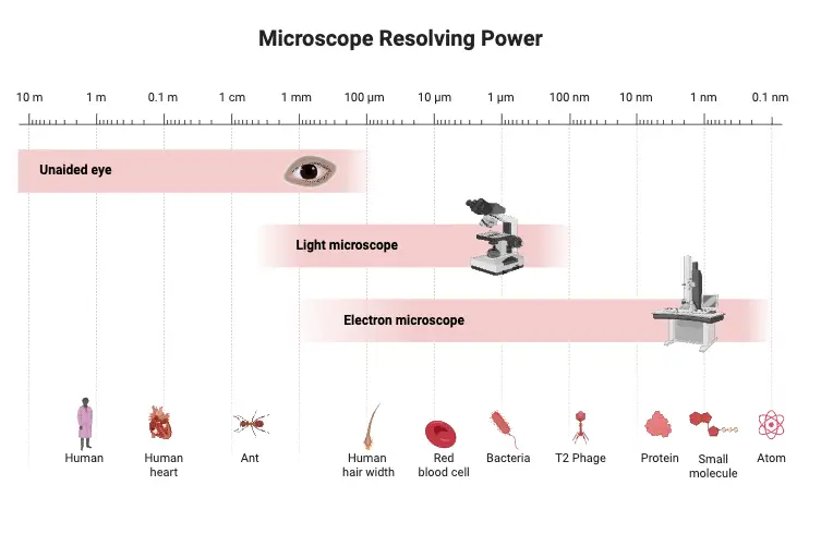
Principle of Electron Microscope – How does an electron microscope work?
- The principle of an electron microscope revolves around the interaction between an electron beam and the specimen under examination, enabling detailed analysis of the specimen’s structure, morphology, and composition.
- The process begins with an electron gun, a critical component that generates the stream of electrons necessary for imaging. These electrons are then directed into a tight, focused beam by two sets of condenser lenses. This beam is further refined as it passes through the specimen, which must be extremely thin—approximately 200 times thinner than those used in optical microscopy. Typically, ultra-thin sections ranging from 20 to 100 nanometers are prepared and placed on a specimen holder for examination.
- To move the electrons efficiently down the microscope column, an accelerating voltage, usually between 100 kV and 1000 kV, is applied between the tungsten filament and the anode. This voltage propels the electrons with high energy towards the specimen.
- As the electron beam passes through the specimen, it interacts with different regions depending on the thickness and refractive index. Denser areas within the specimen scatter more electrons, resulting in fewer electrons reaching the screen. Consequently, these regions appear darker in the final image. Conversely, more transparent areas scatter fewer electrons, allowing more to strike the screen, and thus, appear brighter in the image.
- After interacting with the specimen, the electron beam travels to the objective lens, which is highly powerful and responsible for forming an intermediate magnified image of the specimen. Finally, the ocular lenses further magnify this image, providing a detailed visualization of the sample.
Operating Procedure of Electron microscope
The operating procedure of an electron microscope varies depending on the specific type of electron microscope being used and the sample being studied. However, there are some general steps that are common to most electron microscopes:
- Prepare the sample: The sample must be prepared in a specific way before it can be studied with an electron microscope. This may involve thinning the sample, adding a contrast agent, or mounting the sample on a holder or a stage.
- Position the sample: The sample is placed in the electron beam and is positioned so that the area of interest is in the field of view. The sample may be moved and rotated to view different areas or to focus on specific features.
- Adjust the electron beam: The energy and intensity of the electron beam may be adjusted to optimize the image contrast and to minimize sample damage. The beam may also be focused or rastered over the sample to create a high-resolution image.
- Collect and process the image data: The electrons that are scattered or reflected by the sample are detected by an electronic detector and are used to create an image of the sample. The image data may be processed and analyzed using specialized software.
- View and analyze the image: The image is displayed on a screen or captured by a camera and can be viewed and analyzed to study the structure and properties of the sample. The image may be magnified, rotated, or enhanced to highlight specific features or to aid in the analysis.
Parts of an Electron Microscope
Electron Microscopes contain these following parts;
An electron microscope is a sophisticated instrument composed of several critical components, each playing a vital role in its operation. Below is an overview of the key parts:
- Electron Gun
- The electron gun is the source of the electrons used for imaging. It consists of a heated tungsten filament, which generates a stream of electrons when energized. These electrons are then accelerated towards the specimen.
- Electromagnetic Lenses
- Condenser Lenses: These lenses focus the electron beam onto the specimen. The first condenser lens narrows the beam, while the second forms it into a thin, tight stream for precise interaction with the specimen.
- Objective Lens: After passing through the specimen, the electron beam is directed to the objective lens, which has high magnification power and creates an intermediate image.
- Projector (Ocular) Lenses: These lenses further magnify the intermediate image produced by the objective lens, resulting in the final image. Each set of lenses plays a crucial role in maintaining high resolution and detail throughout the magnification process.
- Specimen Holder
- The specimen holder is designed to securely hold the sample in place during imaging. Typically, it consists of an extremely thin film of carbon or collodion, supported by a metal grid. This setup ensures that the sample remains stable while interacting with the electron beam.
- Image Viewing and Recording System
- The final magnified image is projected onto a fluorescent screen for viewing. Beneath this screen, a camera is often positioned to capture and record the image, allowing for further analysis and documentation.
- Detector
- The detector is a crucial component used to capture electrons that are scattered or reflected by the sample. Various types of detectors can be employed, including scintillators, phosphor screens, and charge-coupled devices (CCDs). These detectors play a significant role in creating a detailed image of the specimen.
- Electronics and Computer System
- This system is responsible for controlling the electron microscope’s operation and processing the data. It typically includes a computer, monitor, and specialized software for managing the microscope’s functions and analyzing the resulting images.
| No. | Part | Description |
|---|---|---|
| 1 | Electron Gun | Generates and accelerates electrons for imaging. In TEM, it consists of a cathode and an anode; in SEM, it has a cathode for generation and an anode for acceleration of electrons. |
| 2 | Electromagnetic Lens System | Comprises different types of lenses to focus and magnify the electron beam: <br> – Condenser lens: Focuses the electron beam on the specimen. <br> – Objective lens: Magnifies the image after the beam passes through the specimen. <br> – Projector (ocular) lenses: Further magnifies the intermediate image to form the final image. |
| 3 | Sample Holder/Specimen Holder | A platform with a mechanical arm to hold and position the specimen. In TEM, the sample is placed on a grid or holder; in SEM, it’s mounted on a stage that can be moved and positioned under the electron beam. |
| 4 | Image Viewing and Recording System | Projects the final image of the specimen onto a fluorescent screen, with a camera located below the screen to record the image. |
| 5 | Detector | Detects scattered or reflected electrons from the sample to create an image. Various types of detectors can be used, including scintillators, phosphor screens, and CCDs. |
| 6 | Electronics and Computer System | Controls the microscope’s operation and processes and displays image data. This system may include computers, monitors, and software for microscope control and data analysis. |
Types of Electron microscope
Electron Microscopes are divided into three classes;
1. Transmission Electron Microscope (TEM)
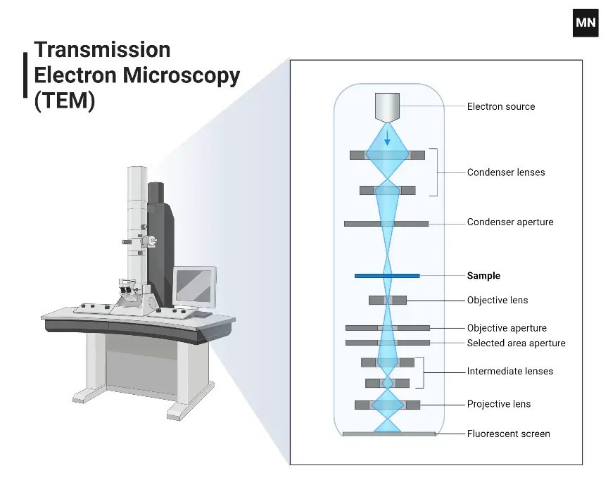
The Transmission Electron Microscope (TEM) is a sophisticated imaging tool that provides detailed internal images of thin specimens by passing a beam of electrons through them. This method allows for high-resolution visualization of samples at the nanoscale.
- Electron Beam Generation
The TEM utilizes a high-voltage electron beam generated by an electron gun, which comprises a tungsten filament known as the cathode. This electron beam is accelerated by an anode, typically set at +100 keV, though it can range from 40 to 400 keV, depending on the requirements of the imaging. - Sample Preparation and Placement
The specimen is carefully prepared to be extremely thin, often only a few nanometers thick, to allow electrons to pass through. It is then placed on a specimen holder or grid within the microscope. - Focusing the Electron Beam
The electron beam is focused onto the specimen using both electrostatic and electromagnetic lenses. These lenses control the beam’s trajectory, ensuring that it passes through the specimen with precision. - Transmission and Scattering
As the electron beam traverses the specimen, it interacts with various components of the sample. Electrons are either transmitted through regions that are partially transparent or scattered by denser areas. This differential transmission and scattering provide contrast in the resulting image. - Magnification and Imaging
The transmitted electrons are then magnified by the objective lens system of the TEM. This magnification process enhances the image’s detail and resolution. The magnified image is projected onto a fluorescent viewing screen, which is coated with a phosphor or scintillator material such as zinc sulfide. - Image Capture and Display
The final image is captured using a digital camera. This recorded image allows for detailed analysis of the specimen’s internal structure, including cellular components, protein molecules, and molecular arrangements. - Applications and Usefulness
TEM is widely used across various fields such as materials science, biology, and nanotechnology. It is instrumental in studying the internal structure of cells, analyzing protein and virus structures, and examining material defects and impurities. The high resolution provided by TEM makes it a powerful tool for observing objects at the atomic and molecular levels.
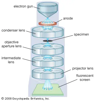
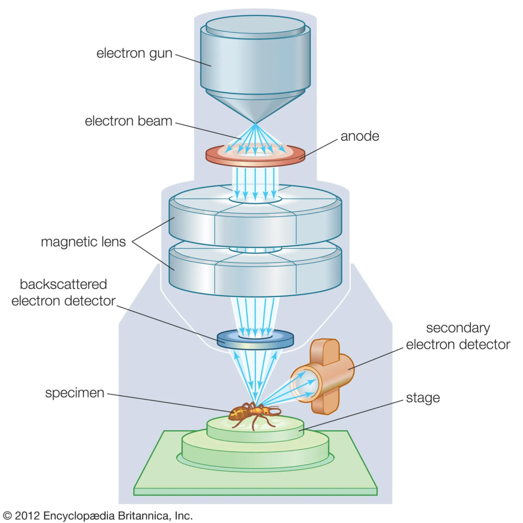
2. Scanning electron microscope (SEM)
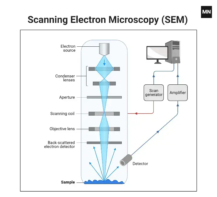
The Scanning Electron Microscope (SEM) is a type of electron microscope that provides detailed images of the surface of specimens. It operates by scanning a focused electron beam across the specimen and analyzing the emitted secondary electrons to create high-resolution images.
- Electron Beam Generation
The SEM begins with a heated electron gun that releases a narrow, focused beam of electrons. This beam is crucial for the imaging process, as it interacts with the specimen’s surface. - Specimen Exposure and Scanning
The specimen is exposed to the narrow electron beam, which scans its surface in a raster pattern. This scanning process involves moving the electron beam rapidly over the specimen to ensure comprehensive coverage. - Secondary Electron Emission
As the electron beam interacts with the specimen, it causes the emission of secondary electrons and other forms of radiation from the specimen’s surface. The amount and intensity of these secondary electrons are influenced by the surface’s shape and chemical composition. - Detection and Signal Conversion
A detector collects the emitted secondary electrons. These electrons are converted into electronic signals, which are then processed to create an image. The detector’s efficiency and accuracy are critical for capturing detailed surface features. - Image Formation and Recording
The electronic signals are scanned and displayed on a cathode ray tube (CRT), similar to a television system. This CRT image is then recorded, either directly from the CRT or by using a digital camera in modern SEMs. - Applications and Advantages
SEM provides high depth of field and detailed surface images, making it highly effective for examining the surfaces of cells, organisms, and various materials. Additionally, SEM is used for particle counting, size determination, and process control, offering capabilities beyond those of Transmission Electron Microscopy (TEM).
3. Scanning and Transmission Electron Microscope (STEM)
The Scanning Transmission Electron Microscope (STEM) integrates the principles of both scanning and transmission electron microscopy, offering a versatile approach to imaging at the nanoscale. STEM combines the strengths of Transmission Electron Microscopes (TEMs) and Scanning Electron Microscopes (SEMs) to provide comprehensive imaging capabilities.
- Electron Beam and Sample Interaction
STEMs utilize a finely focused beam of electrons, which is transmitted through a thin sample. As the electron beam interacts with the sample, it is scattered by the various atomic layers within the material. This scattering process is crucial for obtaining detailed information about the internal structure of the specimen. - Detection of Scattered Electrons
The scattered electrons are captured by an electronic detector positioned to collect these emissions. This detection system converts the scattered electrons into electronic signals, which are then used to construct an image of the sample. The resulting image is displayed on a screen or recorded by a camera. - High-Resolution Imaging
STEM excels in producing high-resolution images of both the surface and internal structures of samples. This capability is particularly valuable for materials with high atomic numbers, such as metals and semiconductors, where detailed imaging of fine structural details is essential. - Sample Sensitivity and Energy Adjustment
One of the advantages of STEM is its ability to study samples that are sensitive to high-energy electrons. The electron beam’s energy can be finely tuned to minimize damage to delicate samples, making STEM suitable for examining materials that might be affected by more intense electron bombardment. - Scanning Mechanism
In a STEM, the specimen is mounted on a stage and scanned by the focused electron beam in a raster pattern. This scanning process ensures that the entire surface of the sample is examined. The interaction of the beam with the sample generates detailed information, which is then used to create the image. - Applications
STEM is employed across various fields, including materials science, nanotechnology, and biology. It is effective for analyzing a wide range of samples, including metals, semiconductors, polymers, and biological materials. The technique is especially useful for identifying structural defects, impurities, and material properties at the atomic level.
4. Other types of Electron Microscope
Besides the commonly used Scanning Electron Microscope (SEM), Transmission Electron Microscope (TEM), and Scanning Transmission Electron Microscope (STEM), several other specialized types of electron microscopes provide unique capabilities and advantages for various scientific applications.
- Reflection Electron Microscope (REM)
- Principle: The Reflection Electron Microscope employs an electron beam that is directed onto the surface of a specimen. The microscope then detects the reflected beam of elastically scattered electrons.
- Techniques: REM is often coupled with Reflection High-Energy Electron Diffraction (RHEED) and Reflection High-Energy Loss Spectroscopy (RHELS). These techniques enhance the analysis of surface structures and provide detailed information about surface morphology and crystallography.
- Scanning Transmission Electron Microscope (STEM)
- Principle: STEM combines features of both SEM and TEM. It rasters a focused electron probe across a thin specimen, detecting electrons that are scattered through the sample.
- Function: This method allows for high-resolution imaging of both surface and internal structures. The technique is particularly valuable for analyzing samples at the nanoscale and minimizing damage to sensitive materials by adjusting the electron beam’s energy.
- Scanning Tunneling Microscope (STM)
- Principle: STM uses a conductive tip held at a voltage that is brought close to the surface of a sample. The tunneling probability of electrons between the tip and the sample, which varies with distance, is used to obtain a profile of the surface.
- Application: This technique is highly effective for imaging surfaces at the atomic scale. It provides detailed topographical information and is used extensively in surface science and nanotechnology.
- Environmental Electron Microscopes
- Principle: Environmental electron microscopes are designed to observe samples in their natural environments, such as within a gas or liquid. They allow for the study of materials under realistic conditions.
- Function: This type of microscope is essential for analyzing materials that are sensitive to vacuum conditions, which are typically required by other electron microscopes. It enables the observation of samples in conditions that closely mimic their natural state.
- Low-Energy Electron Microscopes (LEEMs)
- Principle: LEEM utilizes a beam of low-energy electrons to image the surface of a sample. This technique is particularly beneficial for studying samples that are sensitive to high-energy electrons.
- Application: LEEM is useful for examining organic materials and biological samples. It provides high-resolution images of surfaces without causing significant damage to the specimens.
Differences Between Scanning Electron Microscope (SEM), Transmission Electron Microscope (TEM), and Scanning Transmission Electron Microscope (STEM)
| Feature | Scanning Electron Microscope (SEM) | Transmission Electron Microscope (TEM) | Scanning Transmission Electron Microscope (STEM) |
|---|---|---|---|
| Principle of Imaging | Scans a focused electron beam across the specimen surface; detects secondary electrons emitted from the surface. | Transmits a beam of electrons through a thin specimen; detects electrons that pass through the specimen. | Combines scanning of a focused electron probe with transmission through a thin specimen; detects scattered electrons. |
| Sample Thickness | Can image surfaces of bulk samples or thin sections. | Requires very thin samples to allow electron transmission. | Requires thin samples, similar to TEM, but can also analyze surface and internal structure. |
| Resolution | Moderate to high, typically in the nanometer range. | High, with atomic resolution possible. | High, with capabilities for both surface and internal imaging at the atomic scale. |
| Image Formation | Produces 3D images of surface topography. | Produces 2D images of internal structures. | Produces high-resolution images of both surface and internal structures. |
| Electron Interaction | Electrons interact with the surface, generating secondary electrons. | Electrons interact with the entire thickness of the specimen, revealing internal structures. | Electrons interact with both surface and internal structures, depending on the scan. |
| Sample Preparation | Can be less stringent; specimens need to be coated with a conductive layer if insulating. | Requires ultra-thin sections of the specimen, often prepared by slicing. | Requires thin samples similar to TEM, but scanning adds additional requirements. |
| Applications | Surface morphology, particle size, and texture analysis; suitable for bulk samples. | Internal structure of cells, organelles, and molecular arrangements; ideal for thin sections. | High-resolution imaging of both surface and internal features; used for detailed analysis of nanostructures. |
| Image Detection | Detected by secondary electron detectors; images displayed on a screen or recorded. | Detected by transmitted electrons; images displayed on a fluorescent screen or captured by a camera. | Detected by transmitted and scattered electrons; images displayed on a screen or captured by a camera. |
| Sample Environment | Typically operates in a high vacuum; environmental SEMs can study samples in their native state. | Operates in a high vacuum to avoid electron scattering by air; some variants allow partial pressure. | Operates in a high vacuum; specialized STEMs may accommodate samples in different environments. |
Application of Electron Microscopes
Below are the primary applications of electron microscopes:
- Biological Research
- Microorganisms: Electron microscopes enable the detailed examination of microorganisms such as bacteria, viruses, and fungi. This capability has significantly advanced microbiology, leading to improved disease treatment and understanding of pathogenic mechanisms.
- Cellular Structures: TEMs provide insights into the internal architecture of cells, including organelles and molecular complexes. This detailed imaging helps elucidate cellular functions and abnormalities, contributing to fields such as cell biology and medical research.
- Biomolecules: Detailed imaging of large molecules, including proteins and nucleic acids, is possible with electron microscopes. Techniques like negative staining and metal shadowing enhance the visibility of these biomolecules, aiding in structural biology and drug development.
- Materials Science
- Metals and Alloys: Electron microscopes are crucial for analyzing the microstructure of metals and alloys. They assist in identifying defects, grain boundaries, and phase distributions, which are essential for materials engineering and quality control.
- Semiconductors: The semiconductor industry uses electron microscopes to inspect and characterize materials at the nanoscale. This includes assessing the integrity of semiconductor devices and ensuring the quality of manufacturing processes.
- Crystals: STEMs are employed to study the arrangement of atoms in crystals, providing insights into material properties and aiding in the development of new materials with specific characteristics.
- Quality Control and Failure Analysis
- Industrial Applications: Electron microscopes play a critical role in quality control by detecting imperfections, contaminations, and structural anomalies in manufactured products. They are used in various industries, including aerospace, automotive, and electronics, to ensure product reliability and performance.
- Failure Analysis: When materials or components fail, electron microscopes help identify the root causes by examining fracture surfaces, corrosion patterns, and other failure modes. This analysis helps in refining manufacturing processes and improving product design.
- Environmental Science
- Pollutants: Electron microscopes are used to study airborne pollutants, particulates, and environmental samples. This application aids in understanding the impact of pollutants on health and ecosystems.
- Advanced Research and Development
- Nanotechnology: Electron microscopes are instrumental in nanotechnology, where they enable the observation and manipulation of nanoscale materials and devices. This capability supports research in nanomaterials, nanomedicine, and nanofabrication.
Advantages of Electron Microscopes
Below is a detailed examination of their key benefits:
- Very High Magnification
- Capability: Electron microscopes can achieve magnifications far beyond the limits of light microscopes. This high magnification allows for the observation of extremely small structures and fine details within samples.
- Resolution: The high magnification is paired with high resolution, enabling researchers to visualize features at the atomic level. This capability is crucial for studying nanoscale phenomena and materials.
- Incredibly High Resolution
- Resolution Power: Electron microscopes possess superior resolution compared to optical microscopes due to their use of electron beams rather than light. This enables the examination of structures with sub-nanometer precision.
- Detail: The high resolution allows for detailed imaging of internal structures, defects, and molecular arrangements, providing insights that are not possible with lower-resolution imaging techniques.
- Material Rarely Distorted by Preparation
- Sample Integrity: Electron microscopes are designed to minimize sample distortion during preparation. Techniques such as cryo-electron microscopy preserve the native state of biological samples, reducing artifacts that can occur with other methods.
- Accurate Imaging: This preservation of material integrity ensures that the images obtained are accurate representations of the sample, leading to more reliable scientific data.
- Ability to Investigate Greater Depth of Field
- Depth of Field: Electron microscopes can achieve a greater depth of field compared to light microscopes. This means they can image thicker samples with a greater depth of focus, providing a more comprehensive view of the sample’s three-dimensional structure.
- Applications: This capability is particularly useful in materials science and biological research, where understanding the full structure of a sample is critical.
- Diverse Applications
- Versatility: Electron microscopes are versatile tools used across a wide range of fields, including biology, materials science, and nanotechnology. They are employed to investigate cellular structures, materials properties, and nanomaterials.
- Industry and Research: Their applications include quality control, failure analysis, and advanced research, demonstrating their importance in both academic and industrial contexts.
Limitations of Electron microscope
Below is a detailed examination of these disadvantages:
- Inability to Analyze Live Specimens
- Vacuum Requirement: Electron microscopes require a high-vacuum environment to prevent electron scattering by air molecules. Consequently, live specimens cannot be studied, as they must be prepared in a dry, vacuum-sealed state.
- Biological Limitation: This restriction limits the ability to observe dynamic biological processes and interactions in real-time, thus constraining the scope of biological research applications.
- Sample Preparation Challenges
- Ultra-Thin Sections: To allow electron penetration, samples must be cut into extremely thin sections, often requiring extensive preparation. This process involves drying and slicing the specimen, which can introduce artifacts and alter the sample’s natural state.
- Image Artifacts: Artifacts resulting from sample preparation can affect the accuracy of the images. These artifacts necessitate expertise in preparation techniques to minimize their impact and ensure reliable results.
- Cost and Maintenance
- High Expense: Electron microscopes are costly to purchase, build, and maintain. Their complex technology and the need for specialized components contribute to their high price. This can be a significant barrier for research projects with limited budgets.
- Operational Costs: Although running costs may be comparable to other advanced microscopy techniques, the initial investment and ongoing maintenance expenses are substantial.
- Size and Sensitivity
- Bulky Equipment: Electron microscopes are large and cumbersome, requiring substantial space in a laboratory setting. Their size can be a logistical challenge, particularly in facilities with limited space.
- Sensitivity to External Factors: These microscopes are highly sensitive to vibrations and external magnetic fields, which can interfere with their operation. Proper installation and environmental control are necessary to ensure accurate imaging.
- Training Requirements
- Specialized Training: Operating an electron microscope requires extensive training and expertise. Researchers must acquire specialized knowledge to effectively use these instruments and interpret the complex images they produce.
- Operational Expertise: The complexity of the technology means that only well-trained personnel can maximize the potential of electron microscopy and avoid common pitfalls in image acquisition and analysis.
- Black and White Imaging
- Color Limitation: Electron microscopes produce images in black and white, which can limit the immediate visual interpretation of the data. To enhance the visual representation, images must be artificially colorized, which can sometimes lead to misinterpretations.
Why is electron microscope better than light?
Electron microscopes are generally considered to be more powerful and have a higher resolution than light microscopes, which use light to form an image. There are several reasons for this:
- Higher resolution: Electron microscopes have a much higher resolution than light microscopes and can be used to observe objects at the nanoscale. This makes them a powerful tool for studying the structure and properties of materials at the atomic and molecular level.
- Greater depth of field: Electron microscopes have a greater depth of field than light microscopes, which means that they can produce images of objects that have a greater depth or thickness. This makes them useful for studying thick or three-dimensional samples.
- Ability to study a wide range of samples: Electron microscopes can be used to study a wide range of samples, including metals, semiconductors, polymers, and biological materials. They are particularly useful for studying samples that are too small, too transparent, or too opaque to be studied with a light microscope.
- Ability to study samples under a variety of conditions: Electron microscopes can be used to study samples under a variety of conditions, such as in a vacuum, in a gas, or in a liquid. This makes them useful for studying samples that are sensitive to the environment or that need to be studied in their native state.
- Greater contrast: Electron microscopes can produce images with a high level of contrast, which makes it easier to distinguish between different features in a sample. This is especially useful for studying samples with a complex structure or for identifying defects and impurities in materials.
Electron Microscope: Definition, Types, Parts, Application, Advantages, Disadvantages – Video
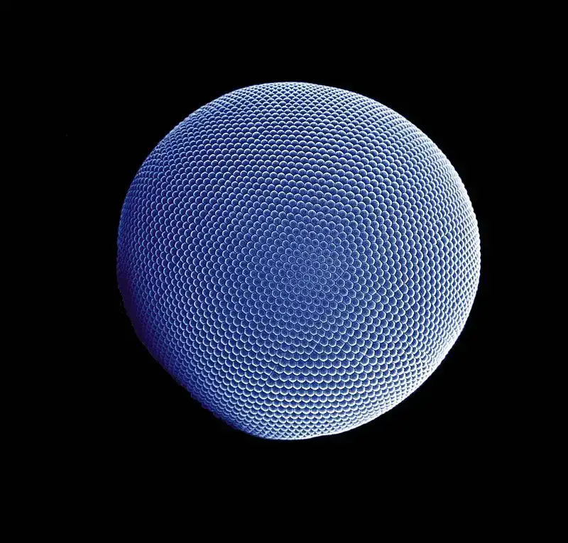
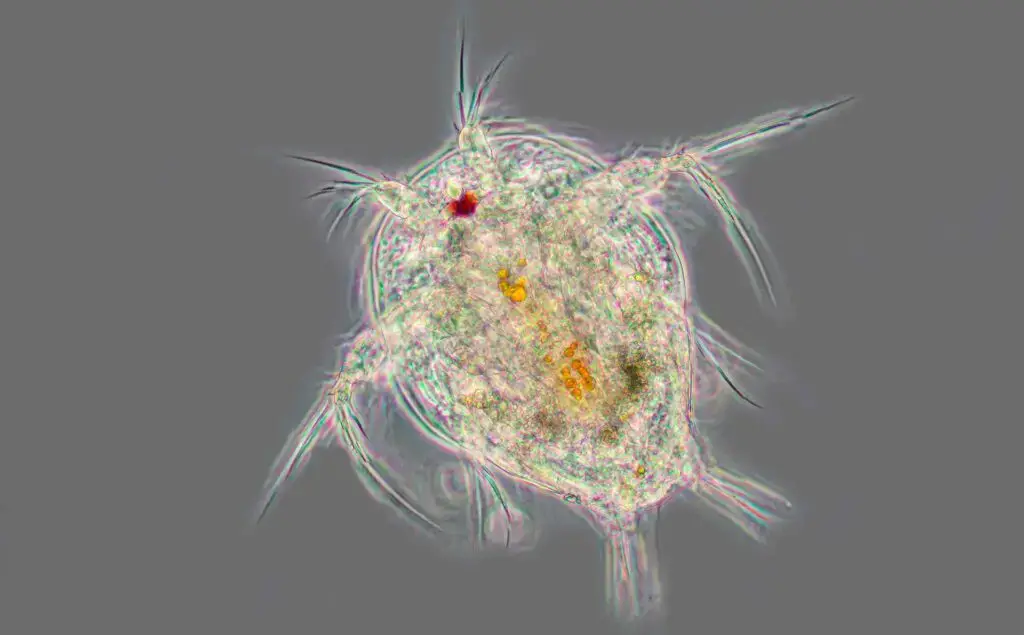
Electron microscope images






Quiz on Electron Microscope
[wp_quiz id=”55660″]
FAQ
What is an electron microscope?
An electron microscope is a type of microscope that uses a beam of electrons to create an image of a sample. Electron microscopes have a higher resolution than optical microscopes, which use light to form an image, and can be used to observe objects that are too small to be seen with an optical microscope. Electron microscopes are used in a variety of fields, including biology, materials science, and nanotechnology, to study the structure and properties of materials at a very small scale. There are several types of electron microscopes, including transmission electron microscopes, scanning electron microscopes, and scanning transmission electron microscopes, each of which has its own unique set of capabilities and applications.
When was the electron microscope invented?
The first electron microscope was developed in the 1930s by German physicist Ernst Ruska and his colleagues at the Technical University of Berlin. Ruska received the Nobel Prize in Physics in 1986 for his work on the development of the electron microscope.
In the early 1930s, Ruska and his colleague Max Knoll developed the first electron microscope, which they called the “transmission electron microscope” (TEM). The TEM used a beam of electrons that was transmitted through a thin sample to create an image of the sample’s internal structure.
In the 1940s, other types of electron microscopes were developed, including the scanning electron microscope (SEM) and the scanning transmission electron microscope (STEM). The SEM used a beam of electrons that was focused onto the surface of a sample to create an image of the sample’s surface features, while the STEM used a beam of electrons that was transmitted through a thin sample and was scattered by the sample as it passed through.
Today, electron microscopes are used in a wide variety of fields to study the structure and properties of materials at the atomic and molecular level. They are an essential tool for scientists and researchers in many fields, including materials science, biology, and nanotechnology.
How much does a electron microscope cost?
The cost of an electron microscope can vary widely depending on the type and capabilities of the microscope. Generally, electron microscopes are more expensive than optical microscopes, due to their higher resolution and specialized features.
A basic transmission electron microscope (TEM) can cost several hundred thousand dollars, while a more advanced TEM with additional features and capabilities can cost several million dollars. A scanning electron microscope (SEM) can also cost several hundred thousand dollars, while a scanning transmission electron microscope (STEM) can cost several million dollars.
In addition to the initial purchase price, there are also ongoing costs associated with operating an electron microscope, including maintenance, repair, and calibration. These costs can vary depending on the type of microscope and the specific needs of the user.
Overall, the cost of an electron microscope can be a significant investment, and it is important to carefully consider the specific needs and budget of an organization when purchasing an electron microscope.
Which lens is used in electron microscope?
Electron microscopes use electron lenses to focus the beam of electrons onto the sample. There are several types of electron lenses that are used in electron microscopes, including:
1. Electromagnetic lenses: Electromagnetic lenses are used in transmission electron microscopes (TEMs) to focus the beam of electrons onto the sample. They consist of a series of electromagnets that bend the path of the electrons and can be used to adjust the focus of the beam.
2. Electrostatic lenses: Electrostatic lenses are used in scanning electron microscopes (SEMs) to focus the beam of electrons onto the sample. They consist of a series of electrostatic plates that are charged to different potentials, which deflect the electrons and focus them onto the sample.
3. Hybrid lenses: Hybrid lenses are a combination of electromagnetic and electrostatic lenses and are used in some types of electron microscopes to focus the beam of electrons onto the sample. Hybrid lenses offer the benefits of both electromagnetic and electrostatic lenses and can be used to achieve a high-resolution image.
In addition to these types of lenses, electron microscopes may also use other types of lenses, such as aberration correctors and condenser lenses, to adjust the focus and contrast of the beam of electrons.
What is the size of electron microscope?
The size of an electron microscope can vary widely depending on the type and capabilities of the microscope. Some electron microscopes are relatively small and portable, while others are large and require a dedicated laboratory space.
Transmission electron microscopes (TEMs) are generally larger than scanning electron microscopes (SEMs) and may require a dedicated laboratory space. TEMs can range in size from a few feet to over 10 feet in length and may weigh several thousand pounds.
Scanning electron microscopes (SEMs) are generally smaller than TEMs and can be more portable. SEMs can range in size from a few feet to several feet in length and may weigh several hundred pounds.
Overall, the size of an electron microscope can vary depending on the specific requirements and needs of the user. Some electron microscopes are designed for use in a laboratory or research facility, while others are designed for use in the field or in a manufacturing environment.
Can electron microscopes see living things?
Unlike light microscopes, electron microscopes cannot be used to directly see living organisms since samples must undergo special preparation before being viewed. Rather, electron microscopes attempt to produce a high-resolution “picture” of a moment in living tissue.
Can electron microscopes see atoms?
Yes, electron microscopes are powerful enough to observe individual atoms and can be used to study the structure and properties of materials at the atomic scale. There are several types of electron microscopes that can be used to study atoms, including transmission electron microscopes (TEMs) and scanning transmission electron microscopes (STEMs).
TEMs and STEMs use a beam of electrons that is transmitted through a thin sample to create an image of the sample’s internal structure. The electrons that pass through the sample are scattered by the atoms in the sample, and the resulting pattern of scattering is used to create an image of the sample.
By analyzing the image, scientists can identify the arrangement of atoms in a sample, measure the distance between atoms, and study the chemical bonding between atoms. Electron microscopes are particularly useful for studying materials that have a complex structure or that are made up of a small number of atoms, such as nanomaterials or thin films.
Overall, electron microscopes are an essential tool for studying the structure and properties of materials at the atomic scale and have played a key role in our understanding of the fundamental properties of matter.
Can electron microscopes see color?
Electron microscopes do not use light to form an image, so they do not produce images with color in the same way that optical microscopes do. Instead, they produce black and white images that show the contrast between different features in the sample.
However, it is possible to assign colors to different features in an electron microscope image to highlight specific structures or to make the image more visually appealing. This is often done using software that can analyze the image data and assign colors to different features based on their size, shape, or position.
For example, scientists may assign different colors to different types of atoms in a sample or to different types of molecules in a cell. This can help to identify specific structures or to study the distribution of different molecules in a sample.
Overall, electron microscopes do not produce images with color in the same way that optical microscopes do, but it is possible to use color to highlight specific features in an electron microscope image to aid in the analysis and interpretation of the image.
How powerful is an electron microscope?
Electron microscopes are very powerful instruments that can be used to study the structure and properties of materials at the atomic and molecular level. They have a much higher resolution than optical microscopes and can be used to observe objects that are too small to be seen with an optical microscope.
The power of an electron microscope is often measured in terms of its resolution, which is the smallest distance between two points that can be distinguished by the microscope. The resolution of an electron microscope is typically measured in nanometers (nm), which is one billionth of a meter.
The resolution of an electron microscope depends on the type of electron microscope being used and the specific sample being studied. Transmission electron microscopes (TEMs) and scanning transmission electron microscopes (STEMs) have a higher resolution than scanning electron microscopes (SEMs) and can be used to study the structure of materials at the atomic scale. TEMs and STEMs can have a resolution of 0.1 nm or less, while SEMs typically have a resolution of around 1-2 nm.
Overall, electron microscopes are very powerful instruments that are essential for studying the structure and properties of materials at the atomic and molecular level. They are used in a wide variety of fields, including materials science, biology, and nanotechnology, to study the structure and properties of materials at a very small scale.
Reference
- https://www.umassmed.edu/cemf/whatisem/
- https://www.microscopemaster.com/electron-microscope.html
- https://www.wikilectures.eu/w/Electron_microscopy/principle
- https://www.biologydiscussion.com/microscope/electron-microscope/electron-microscope-principle-components-specimen-preparation-and-uses/16595
- https://www.slideshare.net/gangahuvin/electron-microscopy-16995175
- https://getrevising.co.uk/grids/electron_microscopes_2
- https://www.yourarticlelibrary.com/microeconomics/working-principle-of-a-electron-microscopes-with-diagram/26479
- https://www.news-medical.net/life-sciences/Advantages-and-Disadvantages-of-Electron-Microscopy.aspx
- https://www.horiba.com/ind/cathodoluminescence-spectroscopy-electron-microscope/
- https://www.hitachi-hightech.com/in/en/products/microscopes/sem-tem-stem/