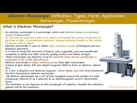
Electron microscope is a high power microscope that uses a beam of accelerated electrons instead of visible light for illumination and image formation. Due to very short wavelength of electrons, it can overcome the diffraction limit of light microscope lenses. Hence, it gives very high resolving power and very high magnification as compared to compound light microscope.
In a light microscope, the magnification is generally limited (about 1000 to 2000×) with a resolution around 200 nm. In electron microscope, magnification can reach up to millions of times and it can resolve very fine details (even near atomic level, around 0.1 nm). The image produced is usually black and white because the detectors record electron signals and not coloured light.
The basic parts include an electron gun (electron source) for producing and accelerating electrons. Electromagnetic lenses are used for focusing and directing the electron beam. A vacuum system is present to avoid collision of electrons with air molecules. Detectors and screen/camera system are used to collect the signals and form the final image.
The common types are Transmission Electron Microscope (TEM) and Scanning Electron Microscope (SEM). TEM allows electrons to pass through an ultra-thin specimen and internal structures are observed. SEM scans the surface of a specimen and gives surface details with 3D like appearance and topographical view.
Electron microscope is used for studying fine structure of cells and tissues, viruses, organelles and ultrastructure. It is also used in material science, semiconductor study, forensic samples and analysis of micro level surface and internal architecture of different specimens.

Principle of Electron Microscope
Principle of Electron Microscope is based on the use of a highly accelerated beam of electrons in place of visible light to produce the image. The electrons have a very short wavelength as compared to light and therefore diffraction limit of glass lenses is avoided. Because of this, very high resolving power and very high magnification is obtained.
In this microscope, electrons are produced from an electron gun (filament like tungsten) by heating or by strong electric field. A high voltage is applied between cathode and anode and the electrons are extracted and accelerated down the column. The electron beam is then focused and controlled by electromagnetic lenses (condenser and objective lenses) which acts like lenses but by magnetic field.
The whole process is carried out in a high vacuum. If air or water vapour is present, electrons get scattered by collision and the beam integrity is lost. When the focused beam strikes the specimen, electrons interact with the material and they may transmit through, get absorbed, or get scattered from surface depending on the type of electron microscope and specimen thickness.
The transmitted or scattered electrons are collected by detectors placed in the chamber. The signal intensity is converted into image contrast and a magnified black and white image is formed. The image is projected on a fluorescent screen or recorded by camera and displayed on monitor.
Operating Procedure of Electron microscope
The following are the steps to be followed for operating an electron microscope.
- In the first step, the vacuum is established inside the microscope chamber. This is done to prevent collision of electrons with gas molecules and also to protect the electron source.
- After vacuum is stable, initial adjustments are made in the microscope. The high voltage, alignment and focusing controls are adjusted for starting the operation.
- In this step, the high voltage is switched off and the specimen is inserted. The specimen holder or cartridge is introduced through an air lock system so that vacuum is not disturbed.
- After the specimen is fixed in position and vacuum is again stabilized, the high voltage is turned on. The electron gun is now allowed to produce the beam for examination.
- The specimen is first viewed at low magnification (about 100× to 1000×) to locate the target area. The required field is selected by moving the stage and beam control.
- The magnification is then increased to observe fine details of the selected area. In SEM, this is achieved by reducing the scanned area on the specimen and focusing the beam properly.
- After imaging is completed, the electron gun is switched off. The cathode is allowed to cool for some time (around 30 minutes) and then the vacuum system is vented safely and specimen is removed.
Parts of an Electron Microscope
The electron microscope is made up of various parts, including
- Electron gun
It is the source of electrons. It generates the electron beam and accelerates it. It consists of filament/cathode, Wehnelt cylinder (grid) for controlling and focusing emission, and an anode for accelerating electrons down the column. - Electromagnetic lenses
These are lenses made by magnetic field and are used to focus and control the electron beam. It includes condenser lenses for producing a narrow beam, objective lens for forming and focusing the image, and projector lenses for increasing final magnification. - Specimen stage and specimen chamber
This is the part where the specimen is placed and held properly. The sample holder/stub is mounted on the stage and it allows positioning of specimen inside the chamber for observation. - Vacuum system
It is used to remove air and gases from the column and specimen chamber. Vacuum is necessary because electrons collide with air molecules and get scattered, so the image gets disturbed. - Apertures
These are small metal apertures placed in the beam path. It blocks stray and scattered electrons and allows only the required aligned beam to pass, improving contrast and clarity. - Detectors and imaging system
These parts collect electrons after interaction with the specimen. It may include electron detectors, fluorescent screen, and digital camera/CCD system. The signals are converted into a black and white image and displayed on screen/monitor.
Types of Electron microscope
The following are the types of electron microscope-
- Transmission Electron Microscope (TEM)
This microscope works by transmission of electrons through the specimen. The specimen is kept ultra-thin. A high voltage electron beam is passed through it. Internal structures are seen. The image is mostly 2D and high resolution. - Scanning Electron Microscope (SEM)
In this microscope, the electron beam is focused into a fine spot. The spot is scanned over the specimen surface. Signals are produced from surface. It gives surface morphology and topography. Image appears 3D like. - Scanning Transmission Electron Microscope (STEM)
This is a combined type of SEM and TEM. A narrow beam is scanned on a thin specimen. Transmitted electrons are collected. Internal detail is obtained with high resolution. - Reflection Electron Microscope (REM)
This microscope uses reflected electrons from the specimen surface. The electrons are elastically scattered and reflected. It is used for surface study. It is useful for crystal surface and topography. - Low-Voltage Electron Microscope (LVEM)
This microscope operates at low accelerating voltage (about 0.5 to 30 kV). It gives increased contrast and less beam damage. It is useful for biological and organic specimens and staining requirement is reduced.


Application of Electron Microscopes
- Forensic science- Used for analysing trace evidences like gunshot residue, paint particles, fibres, blood stains, tool marks, etc.
- Material science and semiconductors- Used for microchip and circuit inspection. Used for measuring small dimensions and detecting very small defects. Used for alloy, coating and nano material study.
- Biological and medical science- Used to view ultrastructure of cells and tissues. Used for bacteria, viruses and organelle study. Used in disease diagnosis related ultrastructure studies.
- Pharmaceutical field- Used in drug research and chemical identification. Used for studying drug target interaction at very high resolution.
- Oil, gas and petroleum industries- Used for porosity study of reservoir rocks. Used for core sample analysis. Used for surface failure analysis of equipment.
- Agriculture and food industry- Used for food particle structure study and contaminant detection. Used for identification of fungi, bacteria, pollen and soil particle study.
- Geology and paleontology- Used for crystal and mineral structure study. Used for microfossil identification.
- Archaeology- Used for examination of ancient soil particles, pigments, bones, teeth, hair, wood and plant remains.
- Steel industry- Used for crack detection and coating defect study. Used for contamination and failure analysis.
- Art- SEM images are used for making digital artworks from highly magnified surface images.
Advantages of Electron Microscopes
- It has very high resolving power because electron wavelength is very small. Hence very fine details which are not seen in light microscope can be seen.
- It gives very high magnification. The magnification can be increased up to very high level (lakhs to millions times) depending on the instrument.
- In SEM, it provides a high depth of field. Surface image looks 3D like and topography is clearly observed.
- It can also be used for elemental and chemical analysis when attached with detectors like EDS/EELS. The elements and their composition can be identified from the same specimen area.
- Both internal and external structures can be studied. TEM gives internal ultrastructure and lattice level details in thin sections, while SEM gives surface morphology of bulk specimens.
- It is used in many fields because of its high power, like biomedical study, forensic work, nanoscience and semiconductor inspection.
Limitations of Electron microscope
- Live specimens cannot be observed. It works under high vacuum and the electron beam is high energy, so biological samples do not survive and they must be dead, fixed and dehydrated.
- Natural colour is not seen. The image is produced in black and white (grey scale) because electrons are detected not light.
- It is very costly. The initial cost is high and maintenance cost is also high (vacuum pumps, calibration, filament change, etc.).
- It needs special facility. It requires a separate room with vibration free setup, controlled power supply and proper HVAC, and also electromagnetic interference should be low.
- Sample preparation is difficult and time consuming. Fixation, dehydration, embedding, ultra-thin sectioning and metal coating are required in many cases.
- Artifacts can be produced. Due to vacuum and preparation steps, shrinkage, collapsing and other changes may occur and the natural structure may be altered.
- Highly trained person is needed. Operating the microscope and preparing good specimen needs skilled personnel.
- Specimen limitation is there. In TEM, the specimen must be very thin (below about 100 nm) for electron transmission. In SEM, the sample should be dry and conductive otherwise charging problem occurs.
Differences Between SEM, TEM and STEM
SEM- It scans the specimen surface by a focused electron beam. Secondary electrons and back scattered electrons are detected for image formation. It gives surface morphology and topography. Image appears 3D like. Specimen can be thick and bulk, only it should fit the chamber. Preparation is simpler, mounting and conductive coating is commonly done. Resolution is about 1 to 10 nm range and magnification is up to about 1 to 2 million times. It works at low accelerating voltage (around 1 to 30 kV).
TEM- It works by transmission of electrons through the specimen. A broad electron beam passes through an ultra-thin section and transmitted electrons are used for image. It gives internal ultrastructure and lattice level details. Image is mainly 2D projection. Specimen must be very thin (about below 100 to 150 nm) so preparation is difficult (fixation, embedding, ultrathin sectioning, staining). Resolution is very high (sub-nanometer to atomic level) and magnification can go up to very high level (even tens of millions). It uses higher accelerating voltage (about 60 to 300 kV).
STEM– It is a combined type of SEM and TEM. A fine beam is focused into a spot and scanned across a thin specimen like SEM. But the image is formed by collecting transmitted electrons like TEM. It gives high resolution internal image and also compositional contrast depending on scattering angle (bright field and dark field type). Specimen must be electron transparent and very thin like TEM. Resolution can be very high (around 100 pm level in advanced system). It is also used with EELS and EDX/EDS for chemical and elemental mapping along with imaging.
Electron Microscope: Definition, Types, Parts, Application, Advantages, Disadvantages – Video
Electron microscope images


Reference
- Averroes AI. (2024, October 30). 3nm & 5nm chip inspection process and tools.
- abberior. (n.d.). Where the tiny becomes mighty: light vs electron microscopy.
- Altobelli, D. E., & Taylor, D. (2024, March 4). Electron gun (beam) systems. Kimball Physics.
- Argonne National Laboratory. (n.d.). Electron and X-ray microscopy (EXM).
- ASU Core Research Facilities. (n.d.). Reflection electron microscopy (REM). Arizona State University.
- Austin. (2024, October 23). Metrology in semiconductor manufacturing. Moov Technologies.
- Choat, B., Jansen, S., & Prychid, C. (n.d.). Preparation of material for TEM examination. PROMETHEUS – Protocols.
- Chui, G. (n.d.). What is cryogenic electron microscopy (cryo-EM)? SLAC National Accelerator Laboratory.
- CIQTEK. (2024, December 5). The differences between scanning electron microscope (SEM) and transmission electron microscope (TEM).
- ConductScience. (2026, February 16). Electron microscopes — Resolution & imaging guide.
- Creative Biostructure. (n.d.). Cryo-EM vs TEM: A comparative analysis.
- Creative Biostructure. (n.d.). Transmission electron microscopy vs. scanning electron microscopy.
- Dondelinger, R. M. (2012). Electron microscopes. Biomedical Instrumentation & Technology, 46(6), 459–463. https://doi.org/10.2345/0899-8205-46.6.459
- Dumančić, E., Vojta, L., & Fulgosi, H. (2023). Beginners guide to sample preparation techniques for transmission electron microscopy. Periodicum Biologorum, 125(1-2), 123–131. https://doi.org/10.18054/pb.v125i1-2.25293
- Electron Microscope. (2012). Types of electron microscopes.
- Electron Optics Instruments. (n.d.). Electron microscope vs. light microscope: A comprehensive…
- Electron Optics Instruments. (n.d.). Electron microscope vs. light microscope: A comprehensive technical comparison for 2026.
- Gujar, S., & Chavan, A. (2026, March). Semiconductor metrology and inspection market, 2035 report. Global Market Insights.
- Güneş, H. (2024, October 23). SEM vs TEM: Electron microscopy technique comparison. Measurlabs.
- hamnamahnoor18. (n.d.). Electron microscope components explained. Scribd.
- Ilitchev, A. (2024). How does an electron microscope work? Thermo Fisher Scientific.
- International Journal of Physics. (n.d.). Applications of nanotechnology in forensic science: A comprehensive review.
- JEOL Ltd. (n.d.). field-emission electron gun, FE electron gun | Glossary.
- Kashi, A. M., Tahermanesh, K., Chaichian, S., Joghataei, M. T., Moradi, F., Tavangar, S. M., Najafabadi, A. S. M., Lotfibakhshaiesh, N., Beyranvand, S. P., Anvari-Yazdi, A. F., & Abed, S. M. (2014). How to prepare biological samples and live tissues for scanning electron microscopy (SEM). Galen Medical Journal, 3(2), 63–80.
- LaGoo, L. (2024). Scanning electron microscopy in forensics (SEM). EBSCO Research Starters.
- Liao, Y. (2006). Field-emission sources. Practical Electron Microscopy and Database.
- Max Planck Institute for Brain Research. (n.d.). Transmission electron microscopy.
- Microscope World. (2026, January 16). Microscopy in semiconductor failure analysis: Techniques, tools, and best practices.
- Microscopy Australia. (n.d.). Electron sources – SEM. MyScope.
- Microscopy Australia. (n.d.). Electron sources – SEM. MyScope.
- Microscopy Australia. (n.d.). High-angle-annular dark-field (HAADF) – TEM. MyScope.
- Microscopy Australia. (n.d.). How the gun works – SEM. MyScope.
- Microscopy Australia. (n.d.). Structure of an SEM – SEM. MyScope.
- Microscopy Australia. (n.d.). TEM – Staining. MyScope.
- Nanoscience Instruments. (n.d.). Scanning transmission electron microscopy.
- Nanoscience Instruments. (n.d.). Thermionic vs. field emission sources: 4 key differences.
- Nanoscience Instruments. (n.d.). What role does SEM play in trace evidence analysis?
- Nanoscience Instruments. (n.d.). What’s the difference between SEM & TEM?
- National Center for Biotechnology Information. (n.d.). Advances in cryo-electron microscopy (cryoEM) for structure-based drug discovery – PMC.
- National Center for Biotechnology Information. (n.d.). Resolution measures in molecular electron microscopy – PMC – NIH.
- r/askscience. (2018). Electron vs light microscope resolution, how does shorter wavelength achieve a higher resolution? Reddit.
- School of the Biological Sciences. (n.d.). Specimen preparation – Electron microscopy. University of Cambridge.
- Science Learning Hub. (2021, March 16). Preparing samples for the electron microscope. The University of Waikato.
- Science Services. (n.d.). Behind the scenes: A look into biological sample preparation for TEM.
- Tescan. (n.d.). Cryo-electron microscopy for life sciences.
- The Department of Physics. (n.d.). Applications of the electron microscope to industry. The University of the West Indies St. Augustine.
- Thermo Fisher Scientific. (n.d.). Electron microscopy | TEM vs SEM.
- Universallab. (2024, June 17). Basic principles and applications of STEM (Scanning transmission electron microscopy).
- University of Gothenburg. (2026, January 29). SEM sample preparation techniques.
- Unknown Author. (n.d.). The electron microscope: Technical principles, architectural design, and multi-disciplinary applications in modern research.
- Wikipedia contributors. (2024, January 8). Wehnelt cylinder. In Wikipedia, The Free Encyclopedia.
- Wikipedia contributors. (2025, December 28). Scanning transmission electron microscopy. In Wikipedia, The Free Encyclopedia.