What is transmission electron microscope?
A transmission electron microscope (TEM) is a high-resolution imaging tool that uses a beam of electrons instead of light to see very small details in thin samples. It can make structures up to several million times bigger, which lets scientists see things like viruses, cell organelles, or even macromolecular complexes. Electrons go through the sample, and the picture is made by how the sample scatters or absorbs them. Unlike light microscopes, TEM gives pictures with much higher resolution because electrons have shorter wavelengths than visible light.
The story starts in 1931, when German scientists Ernst Ruska and Max Knoll made the first model of TEM. Ruska showed that electromagnetic lenses could focus electrons. This led to the idea that electron beams could make an image, just like light does in optical scopes. By 1933, Ruska had made the design better and the resolution better than that of light microscopes. In the 1940s, commercial versions of TEM were made. Since then, it has become one of the most powerful tools in cell biology, virology, and nanotechnology. Over time, modern TEMs have gotten a lot better than the older, bulkier ones. They now have better vacuum systems, digital imaging, cryo-techniques, and more.
Working principle of Transmission Electron Microscope
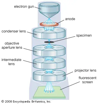
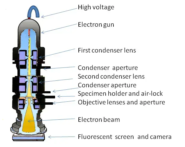
The transmission electron microscope (TEM) works on the same basic ideas as the light microscope, but it uses electrons instead of light to get a much higher resolution. An electron gun sends out electrons, which are then sped up by a high voltage, usually between 80 and 300 keV. This lets them go through very thin samples, which are usually less than 100 nm thick. When the electron beam goes through the sample, it interacts with the atoms inside, which causes the electrons to scatter and pass through. These interactions make the image look different. Areas that are denser scatter more electrons and look darker, while areas that are less dense send more electrons and look lighter. Electromagnetic lenses, like the objective lens, then focus the electrons that have been sent and magnify them through intermediate and projector lenses. This creates an image on a fluorescent screen, photographic film, or digital detector. This imaging process lets you see internal structures with resolutions down to the atomic level, which makes tem a very useful tool for detailed structural analysis in many scientific fields.
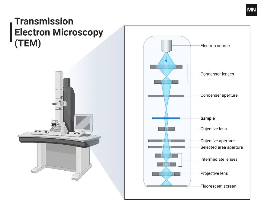
Parts of A Transmission Electron Microscope
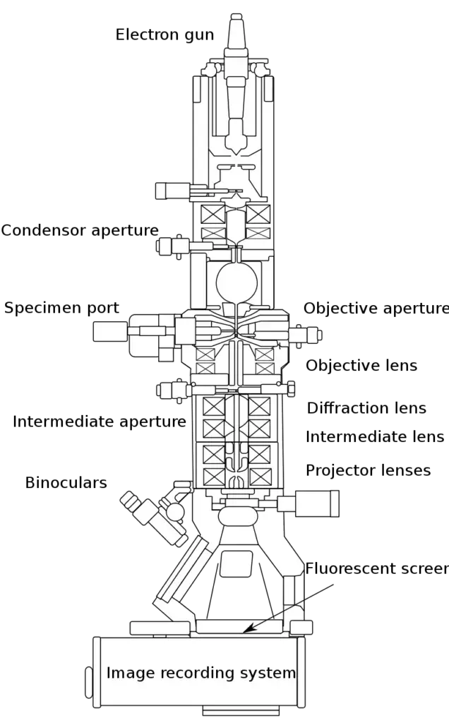
- Electron gun – produces a beam of electrons, typically using a heated tungsten filament or lanthanum hexaboride (LaB₆) crystal.
- Condenser lens system – focuses the electron beam onto the specimen; may consist of one or two lenses to control beam intensity and spot size
- Specimen stage – holds and positions the sample; allows for precise movements in x, y, and z directions, and may include tilting capabilities.
- Objective lens – focuses electrons that have passed through the specimen to form an intermediate image; plays a critical role in determining resolution.
- Intermediate lens – magnifies the intermediate image formed by the objective lens; aids in achieving desired magnification levels.
- Projector lens – further magnifies the image and projects it onto the viewing screen or detector
- Apertures – metallic discs that filter the electron beam; control beam intensity and improve image contrast by eliminating scattered electrons.
- Vacuum system – maintains a high vacuum environment within the microscope column to prevent electron scattering by air molecules; includes roughing and high vacuum pumps.
- Detectors – capture transmitted electrons to form images; can include fluorescent screens, CCD cameras, and direct electron detectors
- Image recording system – converts electron images into a visible format; traditionally used photographic film, now digital systems like CCD or CMOS cameras
- Stigmators – correct optical aberrations such as astigmatism in the electron beam; may be present in condenser, objective, and intermediate stages
- Control console and software – interface for operating the TEM; allows adjustment of parameters like magnification, focus, and alignment
- Specimen preparation tools – include ultramicrotomes for slicing samples into thin sections; essential for biological specimens to be electron-transparent
- Cooling system – maintains low temperatures in detectors and other components to reduce noise and improve image quality
- Electron energy loss spectrometer (EELS) – an optional component for analyzing the energy loss of electrons as they interact with the sample, providing chemical information
- Fluorescent screen – used for real-time viewing of electron images; often coupled with a camera for digital capture
- Power supply – provides the necessary voltage for electron acceleration and lens operation
- Column – the vertical structure housing the electron gun, lenses, and specimen stage; aligned to ensure proper beam path.
- Beam deflectors – electromagnetic or electrostatic devices that manipulate the electron beam’s path for scanning or alignment purposes
- Control electronics – manage the operation of various TEM components, including beam intensity, lens currents, and detector settings.
- Alignment system – ensures that all optical components are correctly aligned to achieve optimal image quality
- Cooling system – maintains low temperatures in detectors and other components to reduce noise and improve image quality.
- Electron energy loss spectrometer (EELS) – an optional component for analyzing the energy loss of electrons as they interact with the sample, providing chemical information.
- Fluorescent screen – used for real-time viewing of electron images; often coupled with a camera for digital capture.
- Power supply – provides the necessary voltage for electron acceleration and lens operation
- Column – the vertical structure housing the electron gun, lenses, and specimen stage; aligned to ensure proper beam path
- Beam deflectors – electromagnetic or electrostatic devices that manipulate the electron beam’s path for scanning or alignment purposes
- Control electronics – manage the operation of various TEM components, including beam intensity, lens currents, and detector settings
- Alignment system – ensures that all optical components are correctly aligned to achieve optimal image quality
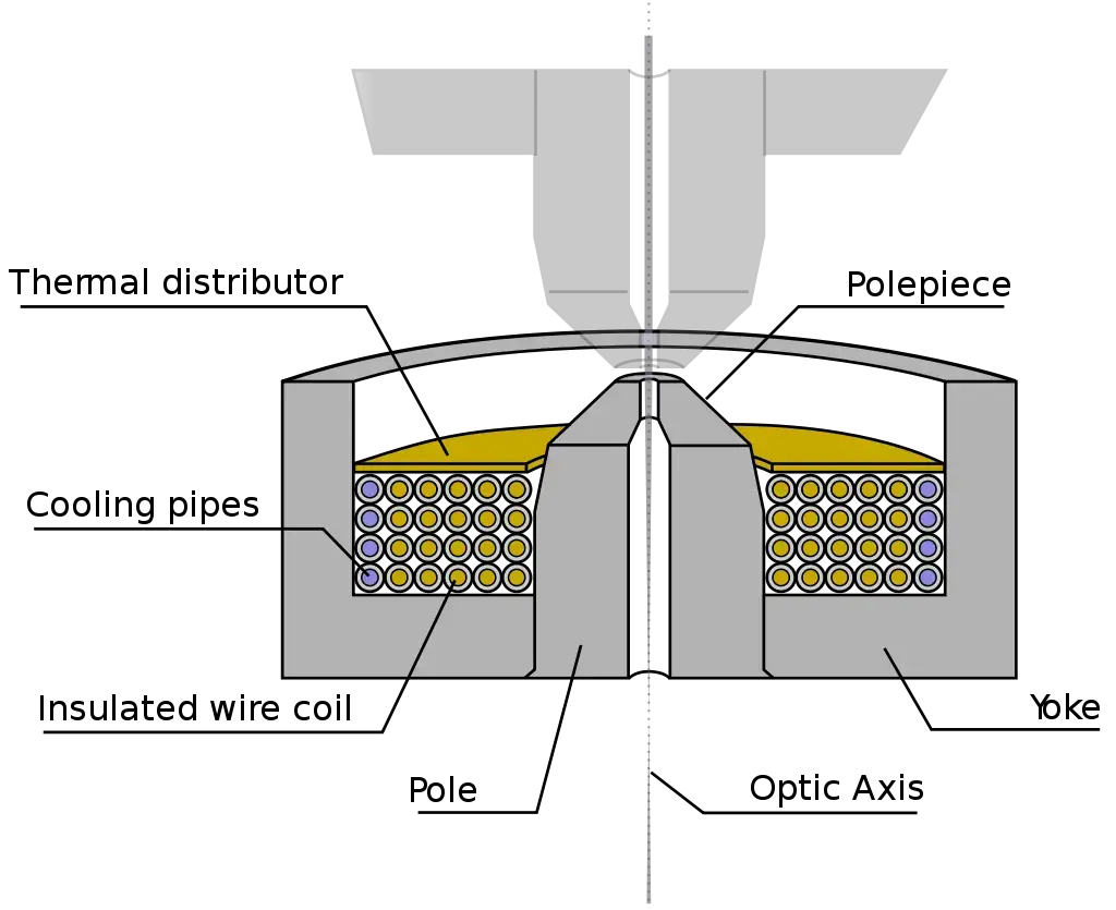
3D Model of Transmission Electron Microscope
How does the transmission electron microscope work?
- An electron gun makes a beam of electrons, usually by heating a tungsten filament or lanthanum hexaboride (LaB₆) crystal.
- The condenser lens system focuses the electron beam on the sample. It may have one or two lenses to change the size of the spot and the strength of the beam.
- The specimen stage holds and moves the sample in the x, y, and z directions with great accuracy. It may also be able to tilt.
- The objective lens focuses electrons that have passed through the specimen to create an intermediate image. This is very important for determining resolution.
- The intermediate lens makes the intermediate image made by the objective lens bigger, which helps you get the right level of magnification.
- The projector lens makes the image even bigger and sends it to the screen or detector.
- Apertures are metal discs that filter the electron beam. They control the beam’s intensity and make the image clearer by getting rid of scattered electrons.
- The vacuum system keeps the microscope column in a high vacuum state so that air molecules don’t scatter electrons. It has both roughing and high vacuum pumps.
- Fluorescent screens, CCD cameras, and direct electron detectors are examples of detectors that capture transmitted electrons to make images.
- The image recording system changes electron images into a form that can be seen. In the past, photographic film was used; now, digital systems like CCD or CMOS cameras are used.
- Stigmators fix optical problems in the electron beam, like astigmatism. They can be found in the condenser, objective, and intermediate stages.
- control console and software interface for running the TEM; lets you change settings like focus, magnification, and alignment
- Ultramicrotomes are tools that cut samples into thin slices. This is important for biological specimens to be electron-transparent.
- The cooling system keeps detectors and other parts at low temperatures to cut down on noise and make the images look better.
- The electron energy loss spectrometer (EELS) is an optional part that can be used to find out how much energy electrons lose when they interact with the sample.
- A fluorescent screen lets you see electron images in real time. It is often used with a camera to take digital pictures.
- The power supply gives the right voltage for speeding up electrons and running the lens.
- column the vertical structure that holds the electron gun, lenses, and specimen stage; it is aligned to make sure the beam path is correct
- Beam deflectors are electromagnetic or electrostatic devices that change the path of an electron beam for the purpose of scanning or alignment.
- Control electronics handle the operation of different TEM parts, such as beam intensity, lens currents, and detector settings.
- The alignment system makes sure that all of the optical parts are lined up correctly so that the image quality is as good as it can be.
Sample Preparation for TEM
TEM sample preparation is intricate and depends on the variety of sample, whether biological or materials, and which properties are studied. TEM sample preparation involves the following:
- Specimen thinness requirement – the specimen must be very thin, about 20-100 nm thick and 0.025-0.1 nm in diameter, similar to bacterial cells, because thick specimens scatter and absorb electrons too much, causing poor visualization
- Chemical fixation – specimen is first fixed with glutaraldehyde or osmium tetraoxide to stabilize and preserve the cell’s original structure
- Dehydration – organic solvents like ethanol are used to completely dehydrate the specimen, preparing it for embedding in plastic
- Embedding in epoxy resin – specimen is permeated with unpolymerized liquid epoxy plastic, which is then hardened to form a solid block, enabling thin section cutting
- Sectioning with ultramicrotome – thin slices are cut from the hardened block using a glass knife mounted on an ultramicrotome, producing sections thin enough for electron transmission
- Staining with heavy metals – thin sections are soaked in lead citrate and uranyl acetate, which bind to cell structures, creating an opaque layer against electrons to increase contrast
- Mounting on copper grids – stained thin sections are placed on copper grids for viewing under the TEM
- Primary staining technique – negative staining combined with heavy metal coating is used, where metallic coating scatters electrons, improving contrast on photographic film, commonly applied for studying bacterial and viral morphology
- Freeze-itching treatment for microbes – to avoid artifacts from chemical fixation and dehydration, microbial cells undergo freeze-itching where specimens are rapidly frozen in liquid nitrogen, cut with precooled knife at -196°C, then warmed at -100°C under vacuum for 2 minutes
- Replica formation – after freeze-itching, specimens are coated with platinum and carbon layers to form replicas that display detailed 3D internal structures under TEM
- Freeze-itching purpose – reduces contamination and artifacts, preserving fine cell structures better than chemical methods
General Operating Procedure of transmission electron microscope
- Gun & vacuum prep – electron gun turned on with high voltage (100–300 kV) and vacuum pumps activated creating ~10⁻⁷–10⁻⁹ Pa low pressure so electrons travel w/o scattering
- Specimen loading – specimen holder loaded using air-lock procedure, ensure O‑ring clean, tilt angles at zero, rotate and insert holder while gun is off and vacuum stable.
- Pump down load‑lock – wait cycles of rough and turbo pumping until gauge green (<~1.3×10⁻⁵ Pa), red light cycles then holder inserted fully by rotation into column.
- Enable beam – press “BEAM” valve open after vacuum ok, adjust brightness to crossover, center beam via X/Y deflectors.
- Align condenser (C2) – overfocus then underfocus C2 lens, center its aperture iteratively using deflectors till beam stays steady on screen center.
- Center & shape beam – use condenser stigmators and deflection coils to round beam and set pivot points for beam tilt/movement alignments.
- Insert apertures & set magnification – select and insert C2, objective & selected-area apertures at desired mag (e.g. 10 k×), adjust intensity and shift to center beam
- Set high tension & spot size – choose HT (e.g. 200 kV) then spot size (2–4) balancing current and beam damage.
- Focus & find ROI – switch to low‑mag, expand beam, use trackball to center, then increase mag, focus with intensity/stigmation, set eucentric height using beam tilt pivot alignments.
- Acquire image – project beam through lenses onto detector (fluorescent screen, CCD, CMOS, film), record image with desired resolution
- Unload specimen – retract apertures, move stage home, close column valve, rotate and extract holder slowly via air‑lock back to atmosphere.
- Shutdown & cleanup – turn off filament/gun, vent vacuum system minimal, remove holder, log session, clean holder and record issues
What is Diffraction Point?
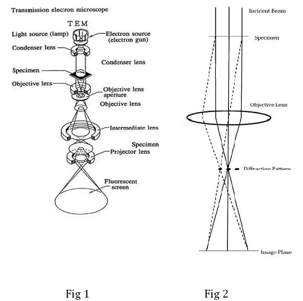
Once the electrons have passed through the specimen, it is found that they scatter because of the electrostatic potential created by the superimposed atoms that make up the specimen. Thus, the electrons that are transmitted pass through an electromagnetic objective lens which, in turn, focuses all of the scattered electrons coming from one point of interest in the specimen to one point of interest in the image plane. Additionally, there is a dotted line in the subsequent image where all of the scattered electrons—those scattered by the specimen in the uniform direction—converge to one point as well. This is called the back focal plane of the objective lens. This is where the diffraction point exists.
Application of Transmission Electron Microscope
- Materials Science – TEM enables atomic-scale imaging of nanomaterials, catalysts, and semiconductors, facilitating the analysis of crystal structures, dislocations, and grain boundaries, crucial for developing advanced materials with tailored properties .
- Nanotechnology – TEM aids in characterizing nanostructures such as quantum dots, nanotubes, and nanowires, providing insights into their size, shape, and structural integrity, essential for the design and application of nanodevices .
- Life Sciences – In structural biology, TEM, particularly cryo-EM, allows for high-resolution visualization of biomolecules like proteins and viruses, contributing to drug discovery and understanding disease mechanisms .
- Semiconductor Industry – TEM is utilized to examine the microstructure of semiconductor devices, identifying defects and ensuring quality control in the fabrication of integrated circuits and microelectronic components .
- Paleontology and Palynology – TEM assists in studying fossilized organic materials and spores, providing valuable information about ancient life forms and environmental conditions .
- Forensic Science – TEM is employed to analyze trace evidence such as gunshot residues and fibers, aiding in criminal investigations by revealing detailed structural information .
- Environmental Science – TEM is used to investigate pollutants and contaminants at the nanoscale, helping to understand their impact on ecosystems and human health .
- Battery Research – TEM provides insights into the microstructure of battery materials, informing the development of more efficient and durable energy storage systems .
- Drug Discovery – TEM facilitates the examination of drug-target interactions at the molecular level, aiding in the design of more effective pharmaceutical compounds .
- Quantum Materials – TEM, particularly aberration-corrected STEM, is instrumental in studying the atomic-scale structure of quantum materials, essential for advancing quantum computing and sensing technologies .
- Catalysis Research – TEM enables the observation of catalyst structures and dynamics at the atomic level, providing insights into reaction mechanisms and aiding in the design of more efficient catalysts .
- In Situ Imaging – Advanced TEM techniques allow for real-time observation of materials under various environmental conditions, enhancing the understanding of dynamic processes such as phase transitions and chemical reactions .
- Structural Biology – TEM is utilized to determine the three-dimensional structures of macromolecular complexes, contributing to the understanding of biological functions and the development of therapeutic strategies .
- Polymer Science – TEM assists in characterizing the morphology and microstructure of polymers, aiding in the development of materials with desired properties for various applications .
- Food Safety – TEM is applied to detect and identify microorganisms and contaminants in food products, ensuring food safety and quality .
- Medical Devices – TEM is used to examine the microstructure of medical implants and devices, ensuring their safety and efficacy .
- Geology – TEM aids in the analysis of mineral structures and compositions, providing insights into geological processes and the formation of natural resources .
- Pharmaceuticals – TEM is employed to study the formulation and stability of pharmaceutical products, contributing to the development of effective drug delivery systems .
- Toxicology – TEM is utilized to examine the effects of toxic substances on cellular structures, aiding in the assessment of environmental and health risks .
- Education – TEM serves as an educational tool in academic institutions, providing students with hands-on experience in advanced microscopy techniques .
- Art Conservation – TEM is applied in the analysis of artworks and artifacts, assisting in the preservation and restoration of cultural heritage .
- Space Science – TEM is used to study extraterrestrial materials and particles, contributing to the understanding of the solar system and beyond .
- Textile Industry – TEM assists in analyzing the fiber structure and composition of textiles, aiding in the development of advanced materials for various applications .
- Aerospace Engineering – TEM is employed to examine the microstructure of materials used in aerospace components, ensuring their performance and reliability .
- Automotive Industry – TEM is used to analyze the materials used in automotive components, contributing to the development of safer and more efficient vehicles .
- Optoelectronics – TEM aids in the study of materials used in optoelectronic devices, facilitating the development of advanced technologies in communication and sensing .
- Marine Biology – TEM is applied to study marine organisms and ecosystems, providing insights into biodiversity and environmental health .
- Agriculture – TEM is used to examine plant cells and tissues, aiding in the development of improved crop varieties and pest-resistant plants .
- Veterinary Science – TEM assists in the diagnosis and study of diseases in animals, contributing to veterinary research and healthcare .
- Human Health – TEM is employed in the study of human cells and tissues, aiding in the diagnosis and understanding of various diseases .
- Regenerative Medicine – TEM is used to study stem cells and tissue engineering, contributing to advancements in regenerative therapies .
- Stem Cell Research – TEM provides detailed images of stem cell morphology and differentiation, enhancing our understanding of stem cell biology .
- Cancer Research – TEM is applied to study the ultrastructure of cancer cells, aiding in the development of targeted therapies .
- Neuroscience – TEM is used to examine neural structures and synaptic connections, contributing to the understanding of brain function and neurological disorders .
- Immunology – TEM assists in studying immune cells and their interactions, providing insights into immune responses and diseases .
- Hematology – TEM is employed to analyze blood cells and their components, aiding in the diagnosis of blood disorders .
- Endocrinology – TEM is used to study endocrine cells and glands, contributing to the understanding of hormonal regulation and related diseases .
- Gastroenterology – TEM assists in examining gastrointestinal tissues, aiding in the diagnosis of digestive system disorders .
- Pulmonology – TEM is applied to study lung tissues, contributing to the understanding of respiratory diseases .
- Nephrology – TEM is used to examine kidney tissues, aiding in the diagnosis of renal diseases .
- Cardiology – TEM assists in studying heart tissues, contributing to the understanding of cardiovascular diseases .
- Hepatology – TEM is employed to analyze liver tissues, aiding in the diagnosis of liver diseases .
- Rheumatology – TEM is used to study joint tissues, contributing to the understanding of autoimmune disorders
Advantages of Transmission Electron Microscope (TEM)
- High resolution—TEM can visualize atomic-level structural details at 0.1 nm. This is useful for studying cell, virus, and nanomaterial ultrastructures.
- High magnification—TEM can magnify structures over 1 million times. Detailed analysis in materials science and nanotechnology requires this.
- TEM supports bright field, dark field, phase contrast, and high-angle annular dark field (HAADF) imaging in scanning transmission electron microscopy (STEM) mode. These modes provide contrast and structural detail.
- TEM collects electron diffraction patterns to provide crystallographic information from nanometer-sized regions. This feature helps analyze material crystalline structure.
- Elemental analysis—TEM uses energy-dispersive X-ray spectroscopy (EDS) to identify and map sample elemental composition for chemical characterization.
- Advanced TEM techniques allow real-time observation of dynamic processes like chemical reactions and phase transitions in controlled environments. This is necessary for in situ material behavior research.
- Sample versatility—TEM can be used on biological tissues, polymers, metals, and semiconductors, making it useful across scientific fields.
- Quantitative analysis—TEM measures particle size distribution and lattice spacing for material characterization and quality control.
- Modern TEM technology allows high-throughput imaging and automation of large sample sets, which is useful for industrial applications.
- Non-destructive analysis – Under certain conditions, TEM can preserve sensitive samples during examination.
Limitations of Transmission Electron Microscope (TEM)
- Extensive sample preparation needed - samples must be ultrathin (<100 nm), embedding, sectioning, staining are time‑consuming, low throughput, and may alter sample structure
- Projection limitation - TEM images are 2D projections of 3D structures so lack depth info and average through thickness, misrepresenting internal variation
- Electron beam damage - high‑energy electrons can damage sensitive materials (esp biological), causing amorphization or structural change before data captured
- Small field of view - typical high‑res TEM image covers only ~100 nm², risking that observed area isn’t representative of whole sample
- Complex image interpretation - images & diffraction patterns require advanced analysis & expertise, not intuitive, risk misinterpretation
- High cost & infrastructure demands - TEM instruments are expensive (US$1–2 M+), need big space, stable environment (vibration, magnetic shielding)
- Specialized training required - advanced operation, sample prep and artifact recognition need skilled operators, lengthy training
- Vacuum and contamination issues - strict vacuum required to avoid scattering & contamination, hydrocarbon deposits degrade quality; maintenance needed arXiv
- Aberrations limit resolution - despite aberration correctors, spherical and chromatic lens defects plus source geometry still impose resolution ceilings
- Massive data generation - especially cryo‑TEM produces terabytes of data per day, requiring HPC infrastructure for storage & processing
Differences between a SEM and a TEM
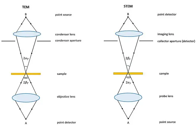
Electron beam source & interaction mode - TEM uses transmitted electrons through ultrathin samples (<100 nm) to project internal structures in 2D, while SEM uses secondary/backscattered electrons from surface interactions to build 3D‑like images by raster scanning
Resolution & magnification - TEM provides much higher resolution (atomic scale, ~0.1 nm) and magnification (up to ~50 million×), SEM resolution is lower (sub‑nm to ~1 nm) and magnification more limited (~2 million× max).
Dimensional info - TEM yields 2D projections lacking surface topology and depth info, SEM gives 3D‑like images with strong depth of field revealing surface texture.
Sample thickness & prep - TEM needs ultrathin (<100 nm) specimens requiring complex prep (thin‑sectioning, embedding, staining), SEM can analyse bulk or thicker samples (mm scale) with minimal prep.8
Infrastructure & cost - TEMs are more expensive and demand sophisticated infrastructure (high vacuum, vibration isolation), SEMs are less costly and simpler to maintain.
Field of view - TEM shows only a small area (~100 nm²) risking unrepresentative sampling, SEM covers larger areas (micrometers to millimeters), better for overview.
Analytical capabilities - TEM can perform diffraction, phase contrast, Z‑contrast, and spectroscopy (EELS/EDS), SEM offers surface compositional analysis like EDS, EBSD, cathodoluminescence.
Beam energy & damage - TEM uses high-energy electrons (80–300 keV) risking sample damage, SEM operates at lower voltages (<20 keV) causing less damage, so more suited for delicate specimens.
Ease of use - SEM operation simpler, less training required; TEM needs high skill for alignment, ultrathin prep, interpretation of complex images.
| Feature | TEM | SEM |
|---|---|---|
| Imaging mechanism | Uses transmitted electrons through an ultrathin (<100 nm) specimen to produce a 2D projection, revealing internal structures | Scans a focused beam across the sample surface; detects secondary/backscattered electrons to produce 3D‑like surface images |
| Resolution | Atomic-scale resolution (~0.05–0.1 nm), enabling visualization of crystal lattices and organelles | Lower resolution (~0.4–1 nm), suitable for detailed surface topography |
| Magnification | Up to ~50 million× | Up to ~2 million× |
| Sample thickness | Requires ultrathin, electron-transparent specimens (<100 nm), requiring complex prep (sectioning, embedding) | Accepts bulk or thicker samples (mm scale); prep often limited to conductive coating |
| Dimensionality of image | 2D internal view; lacks depth information | Provides surface images with strong depth-of-field, conveying a 3D appearance |
| Sample prep complexity | High – ultrathin slicing, staining, vacuum compatibility required | Moderate – simpler prep, mostly conductive coating, faster prep time |
| Operational cost & complexity | More expensive (~US$1–2 M+), requires high vacuum, vibration isolation, specialized operators | Less expensive, easier to operate, fewer environmental constraints |
| Field of view | Small (tens–hundreds nm²), may not represent whole sample | Larger area imaging (µm–mm), better for overview and surveys |
| Analytical capabilities | Internal structure, diffraction patterns, elemental analysis (EELS/EDS), phase contrast | Surface composition, EBSD, cathodoluminescence, EDS elemental mapping |
| Beam damage | High-energy beam (80–300 keV) can damage sensitive specimens | Lower voltages (<20–30 keV) reduce sample damage risk |
| Ease of use | Requires extensive training in alignment, sectioning, artifact interpretation | Simpler controls, quicker to learn and deploy |
Transmission Electron Microscope Definition, Parts, Working Principle, Applications, Advantages – Video
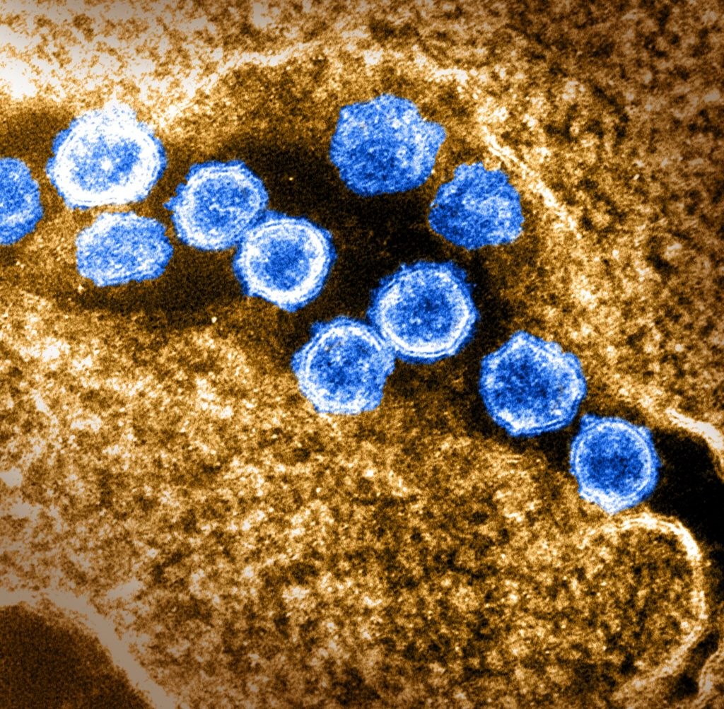
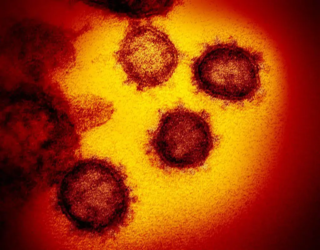
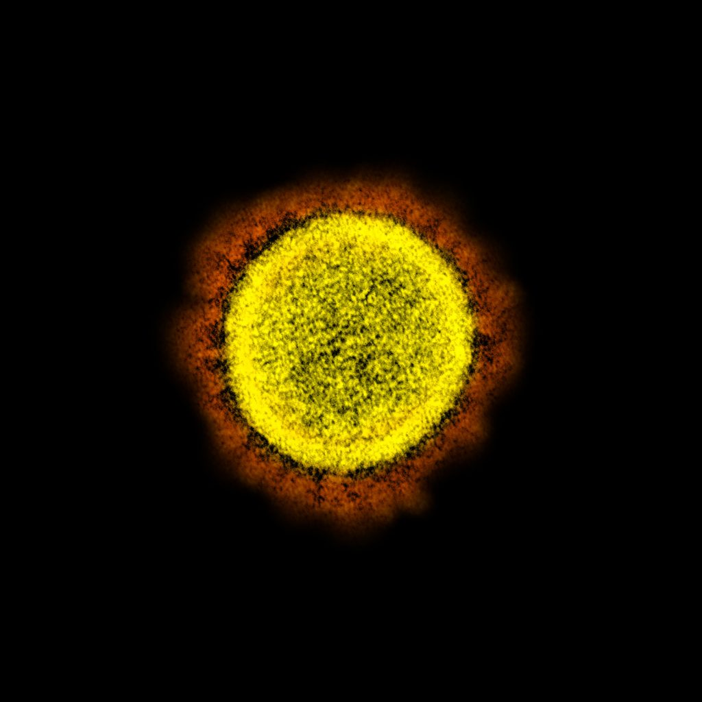
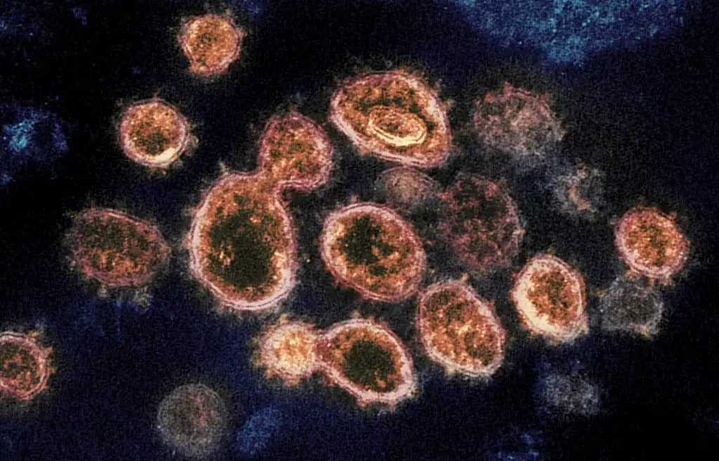
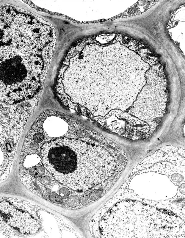
Transmission electron microscope images

- https://www.news-medical.net/life-sciences/Sample-Preparation-in-TEM.aspx
- https://warwick.ac.uk/fac/sci/physics/current/postgraduate/regs/mpagswarwick/
- https://www.jeol.co.jp/en/science/em.html
- https://www.britannica.com/technology/electron-microscope
- https://www.ccber.ucsb.edu/collections-botanical-collections-plant-anatomy/transmission-electron-microscope
- https://www.news-medical.net/life-sciences/What-is-Transmission-Electron-Microscopy.aspx
- https://www.microscopemaster.com/transmission-electron-microscope.html
- https://en.wikipedia.org/wiki/Transmission_electron_microscopy
- https://www.slideshare.net/TakeenKhurshid/transmission-electron
- https://cfamm.ucr.edu/media/161/download?attachment=
- https://www.nanoscience.com/techniques/transmission-electron-microscopy/
- https://www.news-medical.net/life-sciences/Limitations-of-TEM.aspx
- https://pmc.ncbi.nlm.nih.gov/articles/PMC3907272/
- https://pmc.ncbi.nlm.nih.gov/articles/PMC4578338/
- https://www.labx.com/resources/what-is-a-limitation-of-using-electron-microscopes-to-view-specimens/40
- https://www.technologynetworks.com/analysis/articles/electron-microscopy-techniques-strengths-limitations-and-applications-353076