A scanning electron microscope (SEM) produces high-resolution images from an electron beam that scans a focused beam over the surface of a specimen. The benefit of using electrons as opposed to an optical light microscope is that, due to electronegativity, the resultant interactions with the orbitals surrounding the atom create signals that indicate surface morphology and some material information.
This is facilitated by a detector that registers the signals and converts them into quasi-independent visual stimuli. For example, when the beam knocks an atom out of place, secondary electrons are emitted, which an Everhart-Thornley detector can capture. The signal produced is contingent upon the elevation of the various features, which means it is easier to produce images when textures are rough, as more topographical features are rendered.
SEMs have resolutions of < 1 nm, which is useful for assessing grains. Where conventional analytical SEMs operate at high vacuum so that electron scattering does not occur during the imaging of a specimen, there are low vacuum and low humidity options as well as cryogenic and heated options from 0-300° to 500° and above. This means a wide variety of possibilities for certain biological, material, and engineering environments. The SEM was developed over several decades through a collaborative process.
In the 1930s, German physicist Max Knoll postulated that if a beam of electrons were projected, an image would be produced just as with a microscope. He constructed a prototype that validated the hypothesis—but it was not constructed for practical application in the real world. Such challenges were solved by Knoll’s collaborator, Ernst Ruska, who welded electromagnetic lenses. By the 1930s, he could lower electron focusing and take the first direct observational photographs of a specimen. It was Ruska who formalized the technique of transmission electron microscopy (TEM) and won a Nobel Prize in 1986.
More progress was made by American physicist James Hillier. In the 1950s, following the WWII boom and years after much-needed research, Hillier was looking to develop a functioning SEM after much beam focusing and then beam scanning. He created the SEM to rasterize electrons across the surface of a material back and forth, communicating signal strength as signal intensity in three-dimensional space—what SEMs do in the modern day. Hillier would call his device a scanning electron microscope, which also increased opportunities for resolution and use.
Scanning Electron Microscope Definition
A scanning electron microscope (SEM) is a microscope that produces an image of a sample by means of a focused beam of electrons. More specifically, a scanning electron microscope takes pictures of the surface of a sample. The scanning electron microscope is used in all fields—from material science to biology to geology—because it allows researchers to reveal surface properties and evaluate the composition of different materials.
A scanning electron microscope utilizes a beam of electrons emitted from a high-voltage electron gun. This gun aims and focuses the beam through specialized electromagnetic lenses onto the surface of the specimen. As the beam strikes atoms within the specimen, it knocks loose secondary electrons and other types of electromagnetic radiation—most often, X-rays. Detectors capture this data for interpretation and imaging of the specimen surface.
SEMs also have advantages over other microscopes, beyond their stated uses. They can create high quality images at multiple levels of magnification and are known for 3D imaging (i.e., backscattered electron imaging) and compositional analysis (i.e., energy dispersive X-ray spectroscopy [EDS]). Therefore, when it comes to assessing micro level surface morphology and compositional analysis of various materials, SEMs are an appropriate option.
Principle of Scanning Electron Microscope
Whereas the Transmission Electron Microscope relies on electrons that are transmitted through, the Scanning Electron Microscope relies on those that are emitted. The Scanning Electron Microscope runs by giving electrons kinetic energy and then observing the signals produced by the interaction. The emitted electrons are secondary electrons, backscattered electrons, and diffracted backscattered electrons—the last two exist to image crystallized materials—and then photons. However, only secondary and backscattered are applied for imaging purposes. Secondary electrons are applied for imaging purposes since they are emitted from the sample and can give information about sample morphology and topography. Backscattered electrons provide contrast when elemental compositions vary.
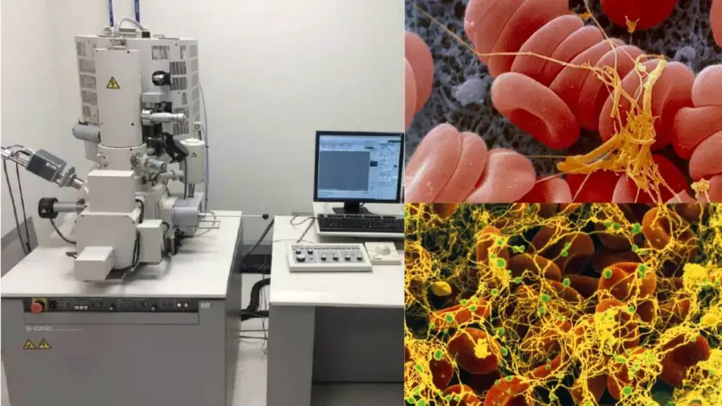
Parts of Scanning Electron Microscope
- Electron Source (Electron Gun): Generates electrons by means of thermionic emission usually via tungsten filament heated from 1-40 kV. A directed subsequent beam of electrons is formed for imaging and analysis. These can be tungsten filaments, lanthanum hexaboride (LaB₆), and field emission guns (FEG).
- Lenses: Uses electromagnetic condenser lenses that reduce the electron beam to a focused spot size. This aids in high resolution since the beam size is focused downward through the column.
- Scanning Coil: Directs the electron beam to move back and forth across the surface of the sample in a raster pattern to systematically image the sample.
- Stage: Keeps sample still and permits x, y, z fine adjustments to focus on specific areas of interest.
- Detectors: Sense outputs such as secondary electrons (SE) and backscattered electrons (BSE). More or less sensitive depending upon beam voltage, sample density, and distance from beam.
- Vacuum System: Produces high vacuum so air molecules do not interrupt the electron path, meaning images are not compromised.
- Display and Control Systems: Interpret signals from detectors and render visualized images. Then, the control systems allow for software control of image magnification, image brightness, beam width, etc.
Sample Preparation for Scanning Electron Microscope
SEM sample preparation is critical for effective imaging and accurate outcomes. While samples may vary (biological, inorganic, powdered, etc.), requiring different preparation approaches, the semi-preparative process generally entails the following:
- Fixation- Either a chemical or stabilizing process to preserve structure. Glutaraldehyde is a frequently used chemical fixative for biological samples. Fixation is critical to successful SEM because if it fails, everything else will fail.
- Dehydration – The process that follows fixation is dehydration of the specimen—especially if biological. This generally occurs through an ethanol series of increasing concentrations up to 100% ethanol. Dehydration is required to prevent imaging artifacts.
- Drying – Excess solvent must be removed to prepare a specimen for the vacuum of the SEM. The customary way to dry a specimen without damage is critical point drying.
- Mounting- After cutting and polishing the sample, to prepare for the imaging process, it should be mounted to a specimen holder or stub with a conductive adhesive. This ensures proper alignment for the imaging process.
- Coating– If non-conductive samples are utilized, they must be sputter coated with gold or gold/palladium. Sputter coating provides a thin film of conductive material over the sample, reducing the charging effect of the electron beam incident upon the sample and increasing imaging quality.
What is causing the sample degradation?
Depending on the acceleration voltage, electrons in the electron beam can interact with electrons within the sample’s atoms. If a valence electron — an electron that can participate in the creation of a chemical bond — is removed from an atom, it will leave behind an electron hole. This vacancy must be filled within 100 femtoseconds (the usual period of an atomic vibration) or the bond will break.
This is not a problem in conductive materials because the electron hole is filled within 1 millisecond (fs). However, it can take many microseconds for non-conductive materials to fill the electron hole, potentially breaking the link and chemically changing the material’s structure.
How does the Scanning Electron Microscope (SEM) work?
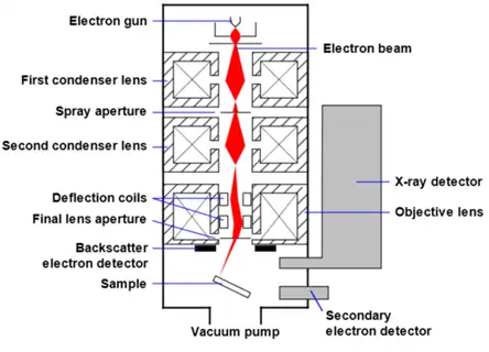
- First, at the top of the SEM column, a heated filament is wired with high voltage in order to create an electron source (or electron gun).
- The electrons travel down the column where they strike a series of magnetic lenses.
- These magnetic lenses are actually solenoids, tubes of electromagnetics wound in a helical pattern. The windings generate surges of voltage which either accelerate or decelerate the electrons, thus arranging for their arrangement as they impact in a tighter or wider beam.
- This subsequently tightened electron beam is aimed at the specimen.
- The SEM is linked to a computer that controls the magnification of the microscope and determines which area will be scanned and replicated.
- The incoming electrons interact with the specimen relative to how much they are slowed down, which is important to note since these electrons have an extremely powerful positive charge before being aimed at the specimen.
- The incoming electrons interact with the specimen and the specimen’s loosely held electrons are ejected from the surface of the specimen.
- The subsequent scattering information collected from this process reveals information about the size, morphology, and composition of the specimen.
- After the interaction of the electron beams and specimen, different varieties of electrons are emitted from the specimen.
- There is an electron detector situated above the specimen, known as the Backscattered Electron (BSE) detector, which detects backscattered electrons. There is an electron detector situated off to the side of the electron chamber, known as the Secondary Electron (SE) detector, which detects secondary electrons that reveal more about the surface.
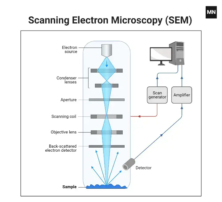
Scanning process and image formation
- In a standard SEM, the electron beam is produced via thermionic emission in an electron gun cathode that consists of a tungsten filament.
- Why tungsten? Tungsten is cheap, has a high melting point, and low vapor pressure. Other types of electron sources include lanthanum hexaboride (LaB6) cathodes usually used in a standard tungsten filament SEM with a change in the vacuum system, and field emission guns (FEG) which are either cold cathode with tungsten single crystal emitters or the thermally excited Schottky type with tungsten single crystal emitters coated with zirconium oxide.
- The electron beam is focused by one or two condenser lenses and operates from 0.2 keV to 40 keV, focused to a pin size of 0.4 nm to 5 nm.
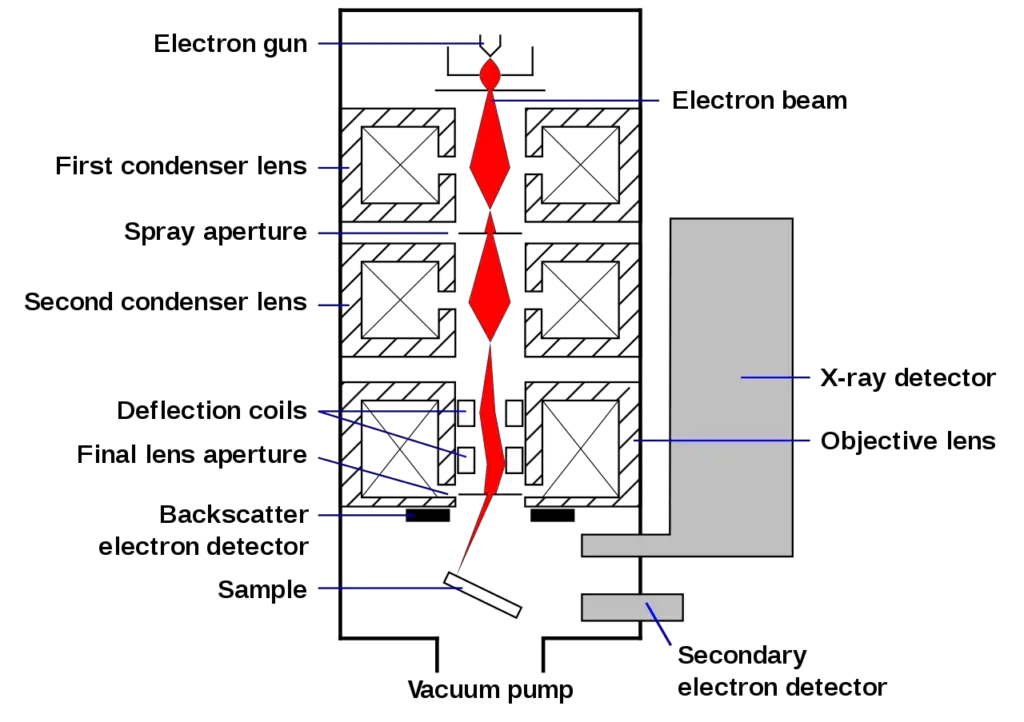
- This happens through either paired scanning coils or paired deflector plates situated in the electron column—the final lens most often—which deflects the beam on the x and y axis so that the beam rasters across a rectangular region at the extreme top of the specimen.
- This happens as the secondary electron beam that exits the material dissipates energy through scattering, and it is emitted in a nonsensical fashion during its engagement within the interaction volume, which can be just under 100 nm to nearly 5 m below the surface.
- The interaction volume is determined by landing energy, atomic number of the material, and density. Specialized detectors can measure the elastic scattering of reflected high-energy electrons, the inelastic scattering of secondary emitted electrons, and emitted x-ray radiation from the energy loss and gain from the particle collision with the sample.
- In addition, the beam current that registers with the sample can be rendered; for example, one can measure and then render the determined beam current sent to the sample and the actual value that the sample registers.
- Such signals—among others—are rendered through various electronic amplifiers, and the variances in levels of intensity are displayed on a computer monitor (cathode-ray tube for older systems).
- Every pixel of computer video memory adds up with the position of the scanning microscope beam moving over the sample, and the final picture shows precisely where, debited, the power exists, away from the scanned portion of the sample. For example, newer microscopes photograph. Older microscopes photograph on film.
Magnification Process
The SEM alters its magnification levels on the order of six—ranging from about 10 to 3,000,000. The ability to achieve such high levels of magnification is different from that of light and transmission electron microscopes. However, it’s also important to note that the final image produced in a SEM is not based on the power of the objective lens.
This is not to say that a SEM doesn’t have an objective lens and a condenser lens; it does—but it’s for focusing the beam down to a point; it does not have to create an image of the specimen. In fact, a SEM can run without an objective lens or a condenser lens; it can run without a condenser lens; however, the electron gun must produce a beam of small enough diameter, yet then the beam will be too monochromatic and resolution will not be as good. SEM magnification, like scanning probe microscopy, is relative to the raster upon the sample and the configuration of the raster of the display screen. Imagining a standard display size, the smaller the sample’s raster, the more magnification occurs and vice versa. Therefore, magnification is only an adjustment of power sent to the x,y scanning coils or the x,y deflector plates, not an adjustment of objective lens power.
How secondary electrons are detected?
The standard imaging mechanism acquires low energy (50 eV) secondary electrons which are emitted from conductor emitter atoms’ valence bands due to inelastic scattering events between the incident beam and the sample. Therefore, the low energy emitted electrons originate from only a few nanometers below the surface of the sample. Those electrons are registered by the Everhart–Thornley detector, a collector-scintillator-photomultiplier-type device.
First, a wire grid electrically biased at ~+400 V gathers secondary electrons; next, the gathered electrons are drawn in and directed toward a scintillator or phosphor setup biased at ~+2,000 V.
These secondary electrons, in their excited state, are enough to excite the scintillator to generate a burst of light (cathodoluminescence) transmitted through a light pipe and a port on the chamber’s side wall to a photomultiplier situated externally to the SEM column.
This altered two-dimensional intensity pattern is subsequently detected by the photomultiplier as an analogue electrical signal, which is transformed from analogue to digital so that it can be observed and saved as a digital file on the analogue video display. This method uses a collimated primary beam that moves while scanning.
The secondary electrons detected vary based on what the detector picks up. However, when the beam hits on-axis to the surface, the interaction volume is radial about the center of the beam and a controlled number of electrons are allowed to “escape” from the surface.
As the angle of incidence increases, the interaction volume increases as well; thus, the “escape” distance from that edge of the beam increases as well, meaning that more secondary electrons are emitted from the sample. Thus, brightened regions occur on vertical edges and raised edges as opposed to the flat—i.e., sometimes the images are almost three-dimensional. Yet clarity of images is possible using the secondary electron signal down to 0.5 nm.

How backscattered electrons are detected?
Backscattered electrons (BSEs) are high-energy electrons that make up the electron beam. Scattering/backscattering occurs via elastic scattering with atoms within the sample interaction volume and beyond. BSEs are used to look at differences in contrast between regions of varying composition because heavy atoms (high atomic number) scatter/backscatter more electrons than light elements (low atomic number), meaning they appear brighter in the micrograph.
The Everhart-Thornley detector—typically fixed off to the side of the sample—doesn’t help with backscattered detection, for an even lower number of those electrons escapes within the solid angle of the detector and, similarly, the positively charged wire mesh of the detector doesn’t have much of an appeal, either, to gather the higher energy BSEs. Thus, special backscatter detectors are located on top of the sample in a “doughnut” approach, concentric with the beam to increase the solid angle of detection.
BSE detectors are standard scintillator or semiconductor. For example, when all quadrants of the detector function to detect electrons in a balanced/fair way about the beam, the artifact generated is fundamental atomic number contrast. However, a more intense topographical contrast comes from the directional BSE detector for back-scattered electrons with an asymmetrical setup off to one side above the sample; the resultant contrast is a slope of topography from that side.
The semiconductor option might have radial quadrants which can be turned on and off, generating different contrasts and directions. The electrons that are backscattered produce an image called electron backscatter diffraction (EBSD) image, which helps determine crystallographic structure.
Resolution of the SEM
Yet where a CCD array or film will always register an image in a SEM, that is not the case for the detector. But material properties are not relative to wavelength, glass lenses or mirrors, or the resolution limits of the detector array as they would be in an optical system. In an electron system, the focusing optics can be far more extensive and simplified in material construction, and the SE detector—essentially measuring current—would be the size of a human fist. Rather, it’s the wavelength of electrons, and the electron-optical system that comprises the scanning beam, that determines the size of the electron dot—and thus the spatial resolution of the SEM. Yet the SEM has so many benefits to compensate for this disadvantage. It can image large areas of the sample, it can image bulk samples (not thin film/foils), and it has myriad analytical modes for compositional and property evaluations. From under 1 nm to over 20 nm. For instance, the latest SEM (30 kV) from 2009 boasts a point resolution of 0.4 nm using a secondary electron detector.
Application of Scanning Electron Microscope
- It is used to examine material microstructure to understand properties in materials science.
- It is used to study cell and tissue morphology for biological research.
- It is used to identify pathogens and test vaccines in medical research.
- It is used to detect and analyze gunshot residue for forensic investigations.
- It is used to conduct failure analysis and ensure quality in industrial processes.
- It is used to analyze minerals’ composition and structure in geological studies.
- It is used to detect art forgeries and study artwork degradation processes.
- It is used to assess water quality in processing, cooling, and wastewater treatment.
- It is used to provide high-resolution imaging for nanomaterials and device development.
- It is used to study pollutant effects and analyze air and water particulate matter.
- It is used to examine soil and plant pathogens to improve crop protection strategies.
Advantages of Scanning Electron Microscope
- They provide high-resolution images of sample surfaces.
- They offer detailed three-dimensional visualizations of surface topography.
- They allow for qualitative elemental analysis.
- It enables examination of thick sections without chromatic aberration.
- It facilitates imaging of uncoated, non-conductive specimens.
- They permit in situ studies of dynamic processes.
- They provide high depth of field for detailed imaging.
- They offer a wide range of magnifications.
- They enable analysis of surface morphology and composition.
- It allows for rapid, automated analysis.
Disadvantages of Scanning Electron Microscope
- They are high equipment and maintenance costs.
- It is required extensive operator training.
- It is complex sample preparation procedures.
- It is limited to analyzing surface structures.
- It is inability to analyze live specimens.
- It is potential for sample damage during analysis.
- Vacuum environment constraints limit sample types.
- Artifacts may occur during sample coating.
- Non-conductive samples need conductive coating.
- It is limited information on internal structures.
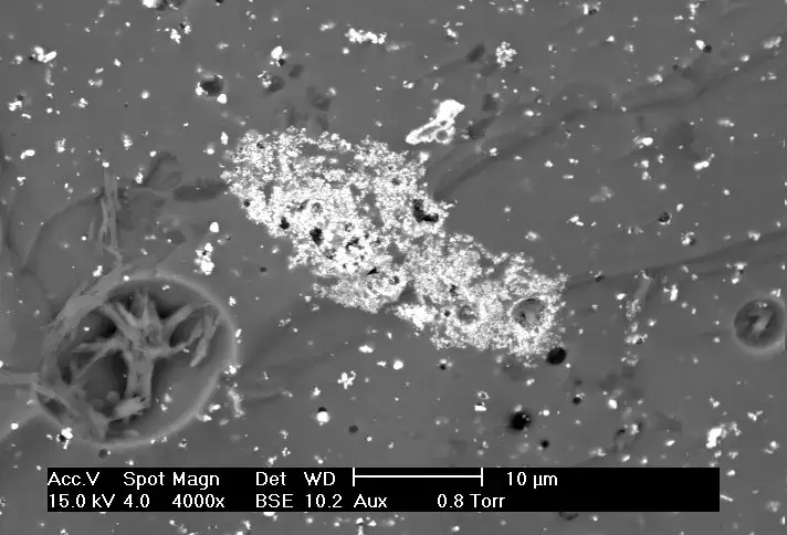
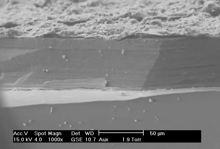
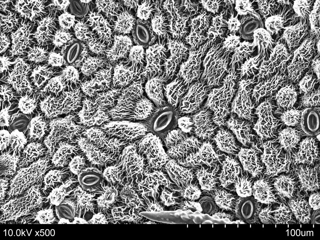
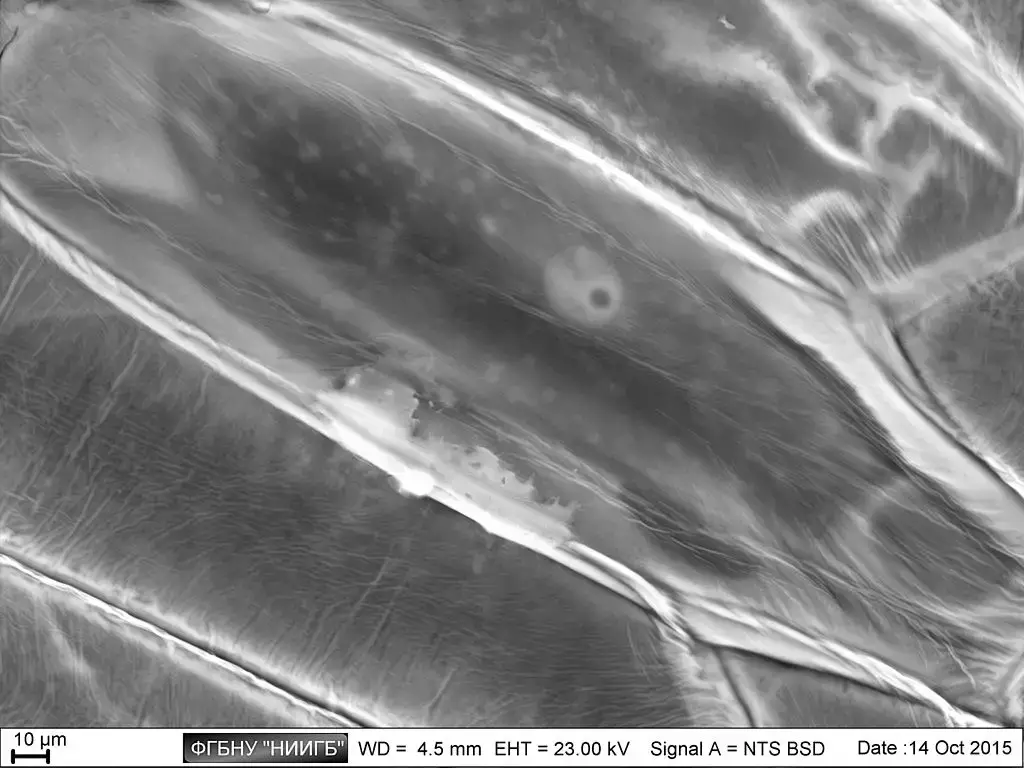
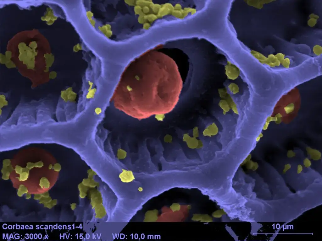
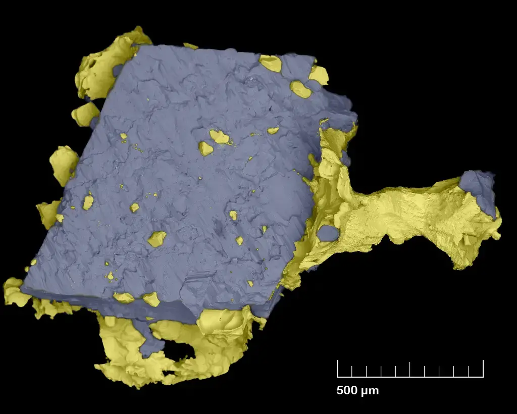
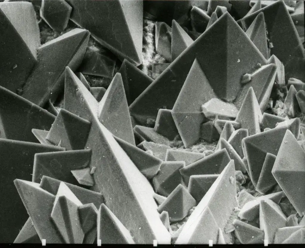
Scanning Electron Microscope (SEM) Images
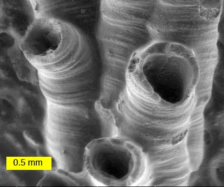
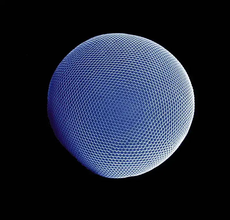


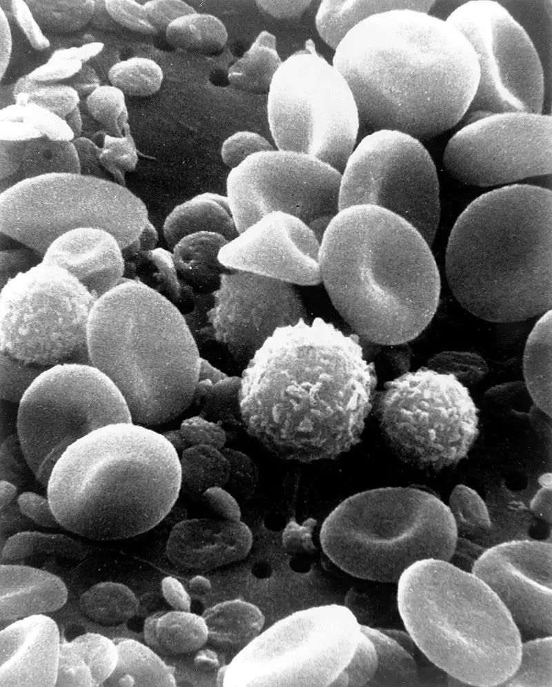
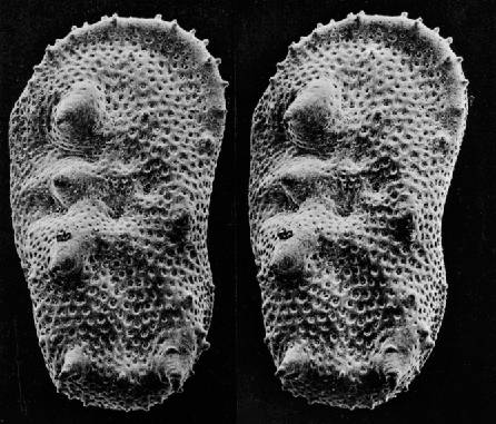



- https://www.microscopemaster.com/scanning-electron-microscope.html
- https://www.atascientific.com.au/sem-imaging-applications-practical-uses-scanning-electron-microscopes/
- https://www.nanoscience.com/techniques/scanning-electron-microscopy/
- https://cf.gu.se/english/centre_for_cellular_imaging/electron-microscopy-
- https://en.wikipedia.org/wiki/Scanning_electron_microscope
- https://www.britannica.com/technology/high-voltage-electron-microscope
- https://www.frontiersin.org/articles/10.3389/fmicb.2020.02014/full
- https://www.atascientific.com.au/sem-imaging-applications-practical-uses-scanning-electron-microscopes/
- https://elementpi.com/sem-disadvantages/
- https://www.news-medical.net/life-sciences/Advantages-and-Disadvantages-of-Electron-Microscopy.aspx
- https://ems-microscopy.com/en/what-are-the-disadvantages-of-sem/
- https://www.innovatechlabs.com/newsroom/2083/advantages-disadvantages-scanning-electron-microscopy/
- https://www.atascientific.com.au/comparing-sem-tem-understanding-the-pros-and-cons/